ZHCSEV0 March 2016 DS90UB921-Q1
PRODUCTION DATA.
- 1 特性
- 2 应用
- 3 说明
- 4 修订历史记录
- 5 Pin Configuration and Functions
-
6 Specifications
- 6.1 Absolute Maximum Ratings
- 6.2 ESD Ratings - JEDEC
- 6.3 ESD Ratings—IEC and ISO
- 6.4 Recommended Operating Conditions
- 6.5 Thermal Information
- 6.6 DC Electrical Characteristics
- 6.7 AC Electrical Characteristics
- 6.8 PCLK Timing Requirements
- 6.9 Recommended Timing for the Serial Control Bus
- 6.10 Switching Characteristics
- 6.11 Typical Charateristics
-
7 Detailed Description
- 7.1 Overview
- 7.2 Functional Block Diagram
- 7.3
Feature Description
- 7.3.1 High Speed Forward Channel Data Transfer
- 7.3.2 Low Speed Back Channel Data Transfer
- 7.3.3 Common Mode Filter Pin (CMF)
- 7.3.4 Video Control Signal Filter
- 7.3.5 EMI Reduction Features
- 7.3.6 LVCMOS VDDIO Option
- 7.3.7 Power Down (PDB)
- 7.3.8 Remote Auto Power-Down Mode
- 7.3.9 Input PCLK Loss Detect
- 7.3.10 Serial Link Fault Detect
- 7.3.11 Pixel Clock Edge Select (TRFB)
- 7.3.12 Frequency Mode Optimizations
- 7.3.13 Interrupt Pins - Funtional Description and Usage (INTB, REM_INTB)
- 7.3.14 Internal Pattern Generation
- 7.3.15 GPIO[3:0] and GPO_REG[7:4]
- 7.3.16 I2S Transmitting
- 7.3.17 Built In Self Test (BIST)
- 7.4 Device Functional Modes
- 7.5 Programming
- 7.6 Register Maps
- 8 Application and Implementation
- 9 Power Supply Recommendations
- 10Layout
- 11器件和文档支持
- 12机械、封装和可订购信息
9 Power Supply Recommendations
9.1 Power Up Requirements and PDB Pin
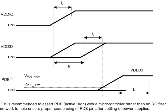
When VDDIO and VDD33 are powered separately, the VDDIO supply (1.8V or 3.3V) should ramp 100us before the other supply, VDD33. If VDDIO is tied with VDD33, both supplies may ramp at the same time. The VDDs (VDD33 and VDDIO) supply ramp should be faster than 1.5 ms with a monotonic rise. If the PDB pin is not controlled by a microcontroller, a large capacitor on the pin is needed to ensure PDB arrives after all the VDDs have settled to the recommended operating voltage. When PDB pin is pulled to VDDIO = 3.0V to 3.6V or VDD33, it is recommended to use a 10 kΩ pull-up and a >10 uF cap to GND to delay the PDB input signal.
A minimum low pulse of 2ms is required when toggling the PDB pin to perform a hard reset.
All inputs must not be driven until VDD33 and VDDIO has reached its steady state value.
 Figure 32. Timing Diagram of DS90UB921-Q1
Table 9. Power-Up Sequencing Constraints
| Symbol | Description | Test Conditions | Min | Typ | Max | Units |
|---|---|---|---|---|---|---|
| VDDIO | VDDIO voltage range | 3.0 | 3.6 | V | ||
| 1.71 | 1.89 | V | ||||
| VDD33 | VDD33 voltage range | 3.0 | 3.6 | V | ||
| VPDB_LOW | PDB LOW threshold Note: VPDB should not exceed limit for respective I/O voltage before 90% voltage of VDD12 |
VDDIO = 3.3V ± 10% | 0.8 | V | ||
| VPDB_HIGH | PDB HIGH threshold | VDDIO = 3.3V ± 10% | 2.0 | V | ||
| t0 | VDDIO rise time | These time constants are specified for rise time of power supply voltage ramp (10% - 90%) | 0.05 | <1.5 | ms | |
| t3 | VDD33 rise time | These time constants are specified for rise time of power supply voltage ramp (10% - 90%) | 0.05 | <1.5 | ms | |
| t1 | VDD33 delay time | VIL of rising edge (VDDIO) to VIL of rising edge (VDD33) The power supplies may be ramped simultaneously. If sequenced, VDDIO should be first.. |
>0 | ms | ||
| t4 | Startup time | The part is powered up after the startup time has elapsed from the moment PDB goes HIGH. Local I2C is available to read/write 921 registers after this time. | <1 | ms |
This device is designed to operate from an input core voltage supply of 3.3V. Some devices provide separate power and ground terminals for different portions of the circuit. This is done to isolate switching noise effects between different sections of the circuit. Separate planes on the PCB are typically not required. Terminal description tables typically provide guidance on which circuit blocks are connected to which power terminal pairs. In some cases, an external filter may be used to provide clean power to sensitive circuits such as PLLs.
9.2 CML Interconnect Guidelines
See AN-1108 (SNLA008) and AN-905 (SNLA035) for full details.
- Use 100Ω coupled differential pairs
- Use the S/2S/3S rule in spacings
- – S = space between the pair
- – 2S = space between pairs
- – 3S = space to LVCMOS signal
- Minimize the number of Vias
- Use differential connectors when operating above 500 Mbps line speed
- Maintain balance of the traces
- Minimize skew within the pair
Additional general guidance can be found in the LVDS Owner’s Manual - available in PDF format from the Texas Instruments web site at: www.ti.com/lvds.