ZHCSF41B December 2015 – March 2021 LMR16030
PRODUCTION DATA
- 1 特性
- 2 应用
- 3 说明
- 4 Revision History
- 5 Pin Configuration and Functions
- 6 Specifications
-
7 Detailed Description
- 7.1 Overview
- 7.2 Functional Block Diagram
- 7.3
Feature Description
- 7.3.1 Fixed Frequency Peak Current Mode Control
- 7.3.2 Slope Compensation
- 7.3.3 Sleep Mode
- 7.3.4 Low Dropout Operation and Bootstrap Voltage (BOOT)
- 7.3.5 Adjustable Output Voltage
- 7.3.6 Enable and Adjustable Undervoltage Lockout
- 7.3.7 External Soft Start
- 7.3.8 Switching Frequency and Synchronization (RT/SYNC)
- 7.3.9 Power Good (PGOOD)
- 7.3.10 Overcurrent and Short Circuit Protection
- 7.3.11 Overvoltage Protection
- 7.3.12 Thermal Shutdown
- 7.4 Device Functional Modes
- 8 Application and Implementation
- 9 Power Supply Recommendations
- 10Layout
- 11Device and Documentation Support
- 12Mechanical, Packaging, and Orderable Information
5 Pin Configuration and Functions
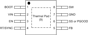
 Figure 5-1 8-Pin (HSOIC)DDA Package(Top View)
Table 5-1 Pin Functions
| PIN | TYPE (1) | DESCRIPTION | |
|---|---|---|---|
| NAME | NO. | ||
| BOOT | 1 | P | Bootstrap capacitor connection for high-side MOSFET driver. Connect a high quality 0.1-μF capacitor from BOOT to SW. |
| VIN | 2 | P | Connect to power supply and bypass capacitors CIN. Path from VIN pin to high frequency bypass CIN and GND must be as short as possible. |
| EN | 3 | A | Enable pin with internal pullup current source. Pull below 1.2 V to disable. Float or connect to VIN to enable. Adjust the input undervoltage lockout with two resistors. See Section 7.3.6. |
| RT/SYNC | 4 | A | Resistor Timing or External Clock input. An internal amplifier holds this pin at a fixed voltage when using an external resistor to ground to set the switching frequency. If the pin is pulled above the PLL upper threshold, a mode change occurs and the pin becomes a synchronization input. The internal amplifier is disabled and the pin is a high impedance clock input to the internal PLL. If clocking edges stop, the internal amplifier is re-enabled and the operating mode returns to frequency programming by resistor. |
| FB | 5 | A | Feedback input pin. Connect to the feedback divider to set VOUT. Do not short this pin to ground during operation. |
| SS or PGOOD |
6 | A | SS pin for soft-start version. Connect to a capacitor to set
soft-start time. PGOOD pin for Power Good version, open drain output for power-good flag. Use a 10-kΩ to 100-kΩ pullup resistor to logic rail or other DC voltage no higher than 7 V. |
| GND | 7 | G | System ground pin |
| SW | 8 | P | Switching output of the regulator. Internally connected to high-side power MOSFET. Connect to power inductor. |
| Thermal Pad | 9 | G | Major heat dissipation path of the die. Must be connected to ground plane on PCB. |
(1) A = Analog, P = Power, G = Ground