ZHCSF49B April   2016  – April 2022 INA301-Q1

PRODUCTION DATA  

  1. 特性
  2. 应用
  3. 说明
  4. Revision History
  5. Pin Configuration and Functions
  6. Specifications
    1. 6.1 Absolute Maximum Ratings
    2. 6.2 ESD Ratings
    3. 6.3 Recommended Operating Conditions
    4. 6.4 Thermal Information
    5. 6.5 Electrical Characteristics
    6. 6.6 Typical Characteristics
  7. Detailed Description
    1. 7.1 Overview
    2. 7.2 Functional Block Diagram
    3. 7.3 Feature Description
      1. 7.3.1 Alert Output ( ALERT Pin)
      2. 7.3.2 Current-Limit Threshold
        1. 7.3.2.1 Resistor-Controlled Current Limit
          1. 7.3.2.1.1 Resistor-Controlled, Current-Limit Example
        2. 7.3.2.2 Voltage-Source-Controlled Current Limit
      3. 7.3.3 Hysteresis
    4. 7.4 Device Functional Modes
      1. 7.4.1 Alert Mode
        1. 7.4.1.1 Transparent Output Mode
        2. 7.4.1.2 Latch Output Mode
  8. Applications and Implementation
    1. 8.1 Application Information
      1. 8.1.1 Selecting a Current-Sensing Resistor
        1. 8.1.1.1 Selecting a Current-Sensing Resistor Example
      2. 8.1.2 Input Filtering
      3. 8.1.3 INA301-Q1 Operation With Common-Mode Voltage Transients Greater Than 36 V
    2. 8.2 Typical Application
      1. 8.2.1 Design Requirements
      2. 8.2.2 Detailed Design Procedure
      3. 8.2.3 Application Curve
  9. Power Supply Recommendations
  10. 10Layout
    1. 10.1 Layout Guidelines
    2. 10.2 Layout Example
  11. 11Device and Documentation Support
    1. 11.1 Documentation Support
      1. 11.1.1 Related Documentation
    2. 11.2 接收文档更新通知
    3. 11.3 支持资源
    4. 11.4 Trademarks
    5. 11.5 Electrostatic Discharge Caution
    6. 11.6 术语表
  12. 12Mechanical, Packaging, and Orderable Information

Alert Output ( ALERT Pin)

The device ALERT pin is an active-low, open-drain output that is designed to be pulled low when the input conditions are detected to be out-of-range. Add a 10-kΩ pullup resistor from ALERT pin to the supply voltage. This open-drain pin can be pulled up to a voltage beyond the VS supply voltage, but must not exceed 5.5 V.

Figure 7-1 shows the alert output response of the internal comparator. When the output voltage of the amplifier is less than the voltage developed at the LIMIT pin, the comparator output is in the default high state. When the amplifier output voltage exceeds the threshold voltage set at the LIMIT pin, the comparator output becomes active and pulls low. This active low output indicates that the measured signal at the amplifier input has exceeded the programmed threshold level, indicating an overcurrent or out-of-range condition has occurred.
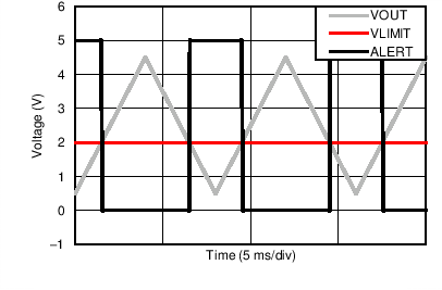
GUID-3AB0B68A-ADC7-4C9A-A317-C09A9E8D8366-low.pngFigure 7-1 Overcurrent Alert Response