ZHCSF96C February 2014 – June 2016 RM57L843
PRODUCTION DATA.
- 1 器件概述
- 2 修订历史记录
- 3 Device Comparison
-
4 Terminal Configuration and Functions
- 4.1 ZWT BGA Package Ball-Map (337 Terminal Grid Array)
- 4.2
Terminal Functions
- 4.2.1
ZWT Package
- 4.2.1.1 Multibuffered Analog-to-Digital Converters (MibADC)
- 4.2.1.2 Enhanced High-End Timer Modules (N2HET)
- 4.2.1.3 RAM Trace Port (RTP)
- 4.2.1.4 Enhanced Capture Modules (eCAP)
- 4.2.1.5 Enhanced Quadrature Encoder Pulse Modules (eQEP)
- 4.2.1.6 Enhanced Pulse-Width Modulator Modules (ePWM)
- 4.2.1.7 Data Modification Module (DMM)
- 4.2.1.8 General-Purpose Input / Output (GIO)
- 4.2.1.9 Controller Area Network Controllers (DCAN)
- 4.2.1.10 Local Interconnect Network Interface Module (LIN)
- 4.2.1.11 Standard Serial Communication Interface (SCI)
- 4.2.1.12 Inter-Integrated Circuit Interface Module (I2C)
- 4.2.1.13 Multibuffered Serial Peripheral Interface Modules (MibSPI)
- 4.2.1.14 Ethernet Controller
- 4.2.1.15 External Memory Interface (EMIF)
- 4.2.1.16 Embedded Trace Macrocell Interface for Cortex-R5F (ETM-R5)
- 4.2.1.17 System Module Interface
- 4.2.1.18 Clock Inputs and Outputs
- 4.2.1.19 Test and Debug Modules Interface
- 4.2.1.20 Flash Supply and Test Pads
- 4.2.1.21 Supply for Core Logic: 1.2-V Nominal
- 4.2.1.22 Supply for I/O Cells: 3.3-V Nominal
- 4.2.1.23 Ground Reference for All Supplies Except VCCAD
- 4.2.1.24 Other Supplies
- 4.2.2 Multiplexing
- 4.2.1
ZWT Package
-
5 Specifications
- 5.1 Absolute Maximum Ratings
- 5.2 ESD Ratings
- 5.3 Power-On Hours (POH)
- 5.4 Device Recommended Operating Conditions
- 5.5 Switching Characteristics over Recommended Operating Conditions for Clock Domains
- 5.6 Wait States Required - L2 Memories
- 5.7 Power Consumption Summary
- 5.8 Input/Output Electrical Characteristics Over Recommended Operating Conditions
- 5.9 Thermal Resistance Characteristics for the BGA Package (ZWT)
- 5.10 Timing and Switching Characteristics
-
6 System Information and Electrical Specifications
- 6.1 Device Power Domains
- 6.2 Voltage Monitor Characteristics
- 6.3 Power Sequencing and Power-On Reset
- 6.4 Warm Reset (nRST)
- 6.5 ARM Cortex-R5F CPU Information
- 6.6 Clocks
- 6.7 Clock Monitoring
- 6.8 Glitch Filters
- 6.9 Device Memory Map
- 6.10 Flash Memory
- 6.11 L2RAMW (Level 2 RAM Interface Module)
- 6.12 ECC / Parity Protection for Accesses to Peripheral RAMs
- 6.13 On-Chip SRAM Initialization and Testing
- 6.14 External Memory Interface (EMIF)
- 6.15 Vectored Interrupt Manager
- 6.16 ECC Error Event Monitoring and Profiling
- 6.17 DMA Controller
- 6.18 Real-Time Interrupt Module
- 6.19 Error Signaling Module
- 6.20 Reset / Abort / Error Sources
- 6.21 Digital Windowed Watchdog
- 6.22
Debug Subsystem
- 6.22.1 Block Diagram
- 6.22.2 Debug Components Memory Map
- 6.22.3 Embedded Cross Trigger
- 6.22.4 JTAG Identification Code
- 6.22.5 Debug ROM
- 6.22.6 JTAG Scan Interface Timings
- 6.22.7 Advanced JTAG Security Module
- 6.22.8 Embedded Trace Macrocell (ETM-R5)
- 6.22.9 RAM Trace Port (RTP)
- 6.22.10 Data Modification Module (DMM)
- 6.22.11 Boundary Scan Chain
-
7 Peripheral Information and Electrical Specifications
- 7.1
Enhanced Translator PWM Modules (ePWM)
- 7.1.1 ePWM Clocking and Reset
- 7.1.2 Synchronization of ePWMx Time-Base Counters
- 7.1.3 Synchronizing all ePWM Modules to the N2HET1 Module Time Base
- 7.1.4 Phase-Locking the Time-Base Clocks of Multiple ePWM Modules
- 7.1.5 ePWM Synchronization with External Devices
- 7.1.6 ePWM Trip Zones
- 7.1.7 Triggering of ADC Start of Conversion Using ePWMx SOCA and SOCB Outputs
- 7.1.8 Enhanced Translator-Pulse Width Modulator (ePWMx) Electrical Data/Timing
- 7.2 Enhanced Capture Modules (eCAP)
- 7.3 Enhanced Quadrature Encoder (eQEP)
- 7.4 12-bit Multibuffered Analog-to-Digital Converter (MibADC)
- 7.5 General-Purpose Input/Output
- 7.6 Enhanced High-End Timer (N2HET)
- 7.7 Controller Area Network (DCAN)
- 7.8 Local Interconnect Network Interface (LIN)
- 7.9 Serial Communication Interface (SCI)
- 7.10 Inter-Integrated Circuit (I2C)
- 7.11 Multibuffered / Standard Serial Peripheral Interface
- 7.12 Ethernet Media Access Controller
- 7.1
Enhanced Translator PWM Modules (ePWM)
- 8 Applications, Implementation, and Layout
- 9 Device and Documentation Support
- 10Mechanical Data
6 System Information and Electrical Specifications
6.1 Device Power Domains
The device core logic is split up into multiple virtual power domains to optimize the power for a given application use case.
This device has six logic power domains: PD1, PD2, PD3, PD4, PD5, and PD6. PD1 is a domain which cannot turn off of its clocks at once through the Power-Management Module (PMM). However, individual clock domain operating in PD1 can be individually enabled or disabled through the SYS.CDDIS register. Each of the other power domains can be turned ON, IDLE or OFF as per the application requirement through the PMM module.
In this device, a power domain can operate in one of the three possible power states: ON, IDLE and OFF. ON state is the normal operating state where clocks are actively running in the power domain. When clocks are turned off, the dynamic current is removed from the power domain. In this device, both the IDLE and OFF states have the same power characteristic. When put into either the IDLE or the OFF state, only clocks are turned off from the power domain. Leakage current from the power domain still remains. Note that putting a power domain in the OFF state will not remove any leakage current in this device. In changing the power domain states, the user must poll the system status register to check the completion of the transition. From a programmer model perspective, all three power states are available from the PMM module.
The actual management of the power domains and the hand-shaking mechanism is managed by the PMM. Refer to the Power Management Module (PMM) chapter of the device technical reference manual for more details.
6.2 Voltage Monitor Characteristics
A voltage monitor is implemented on this device. The purpose of this voltage monitor is to eliminate the requirement for a specific sequence when powering up the core and I/O voltage supplies.
6.2.1 Important Considerations
- The voltage monitor does not eliminate the need of a voltage supervisor circuit to ensure that the device is held in reset when the voltage supplies are out of range.
- The voltage monitor only monitors the core supply (VCC) and the I/O supply (VCCIO). The other supplies are not monitored by the VMON. For example, if the VCCAD or VCCP are supplied from a source different from that for VCCIO, then there is no internal voltage monitor for the VCCAD and VCCP supplies.
6.2.2 Voltage Monitor Operation
The voltage monitor generates the Power Good MCU signal (PGMCU) as well as the I/Os Power Good IO signal (PGIO) on the device. During power-up or power-down, the PGMCU and PGIO are driven low when the core or I/O supplies are lower than the specified minimum monitoring thresholds. The PGIO and PGMCU being low isolates the core logic as well as the I/O controls during power up or power down of the supplies. This allows the core and I/O supplies to be powered up or down in any order.
When the voltage monitor detects a low voltage on the I/O supply, it will assert a power-on reset. When the voltage monitor detects an out-of-range voltage on the core supply, it asynchronously makes all output pins high impedance, and asserts a power-on reset. The I/O supply must be above the threshold for monitoring the core supply. The voltage monitor is disabled when the device enters a low power mode.
The VMON also incorporates a glitch filter for the nPORRST input. Refer to Section 6.3.3.1 for the timing information on this glitch filter.
Table 6-1 Voltage Monitoring Specifications
6.2.3 Supply Filtering
The VMON has the capability to filter glitches on the VCC and VCCIO supplies.
Table 6-2 lists the characteristics of the supply filtering. Glitches in the supply larger than the maximum specification cannot be filtered.
Table 6-2 VMON Supply Glitch Filtering Capability
| PARAMETER | MIN | MAX | UNIT |
|---|---|---|---|
| Width of glitch on VCC that can be filtered | 250 | 1000 | ns |
| Width of glitch on VCCIO that can be filtered | 250 | 1000 | ns |
6.3 Power Sequencing and Power-On Reset
6.3.1 Power-Up Sequence
There is no timing dependency between the ramp of the VCCIO and the VCC supply voltage. The power-up sequence starts with the I/O voltage rising above the minimum I/O supply threshold, (for more details, see Table 6-3), core voltage rising above the minimum core supply threshold and the release of power-on reset. The high-frequency oscillator will start up first and its amplitude will grow to an acceptable level. The oscillator start-up time is dependent on the type of oscillator and is provided by the oscillator vendor. The different supplies to the device can be powered up in any order.
The device goes through the following sequential phases during power up.
Table 6-3 Power-Up Phases
| Oscillator start-up and validity check | 1024 oscillator cycles |
| eFuse autoload | 3650 oscillator cycles |
| Flash pump power-up | 250 oscillator cycles |
| Flash bank power-up | 1460 oscillator cycles |
| Total | 6384 oscillator cycles |
The CPU reset is released at the end of the above sequence and fetches the first instruction from address 0x00000000.
6.3.2 Power-Down Sequence
The different supplies to the device can be powered down in any order.
6.3.3 Power-On Reset: nPORRST
This is the power-on reset. This reset must be asserted by an external circuitry whenever the I/O or core supplies are outside the specified recommended range. This signal has a glitch filter on it. It also has an internal pulldown.
6.3.3.1 nPORRST Electrical and Timing Requirements
Table 6-4 Electrical Requirements for nPORRST

6.4 Warm Reset (nRST)
This is a bidirectional reset signal. The internal circuitry drives the signal low on detecting any device reset condition. An external circuit can assert a device reset by forcing the signal low. On this terminal, the output buffer is implemented as an open drain (drives low only). To ensure an external reset is not arbitrarily generated, TI recommends that an external pullup resistor is connected to this terminal.
This terminal has a glitch filter. It also has an internal pullup
6.4.1 Causes of Warm Reset
Table 6-5 Causes of Warm Reset
| DEVICE EVENT | SYSTEM STATUS FLAG |
|---|---|
| Power-Up Reset | Exception Status Register, bit 15 |
| Oscillator fail | Global Status Register, bit 0 |
| PLL slip | Global Status Register, bits 8 and 9 |
| Watchdog exception | Exception Status Register, bit 13 |
| Debugger reset | Exception Status Register, bit 11 |
| CPU Reset (driven by the CPU STC) | Exception Status Register, bit 5 |
| Software Reset | Exception Status Register, bit 4 |
| External Reset | Exception Status Register, bit 3 |
6.4.2 nRST Timing Requirements
Table 6-6 nRST Timing Requirements(1)
6.5 ARM Cortex-R5F CPU Information
6.5.1 Summary of ARM Cortex-R5F CPU Features
The features of the ARM Cortex-R5F CPU include:
- An integer unit with integral Embedded ICE-RT logic.
- High-speed Advanced Microprocessor Bus Architecture (AMBA) Advanced eXtensible Interfaces (AXI) for Level two (L2) master and slave interfaces.
- Floating-Point Coprocessor
- Dynamic branch prediction with a global history buffer, and a 4-entry return stack
- Low interrupt latency.
- Nonmaskable interrupt.
- Harvard Level one (L1) memory system with:
- 32KB of instruction cache and 32KB of data cache implemented. Both Instruction and data cache have ECC support.
- ARMv7-R architecture Memory Protection Unit (MPU) with 16 regions
- Dual core logic for fault detection in safety-critical applications.
- L2 memory interface:
- Single 64-bit master AXI interface
- 64-bit slave AXI interface to cache memories
- 32-bit AXI_Peri ports to support low latency peripheral ports
- Debug interface to a CoreSight Debug Access Port (DAP).
- Performance Monitoring Unit (PMU).
- Vectored Interrupt Controller (VIC) port.
- AXI accelerator coherency port (ACP) supporting IO coherency with write-through cacheable regions
- Ability to generate ECC on L2 data buses and parity of all control channels
- Both CPU cores in lock-step
- Eight hardware breakpoints
- Eight watchpoints
6.5.2 Dual Core Implementation
The device has two Cortex-R5F cores, where the output signals of both CPUs are compared in the CCM-R5F unit. To avoid common mode impacts the signals of the CPUs to be compared are delayed by two clock cycles as shown in Figure 6-2.
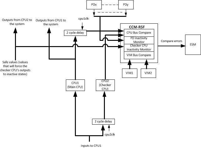 Figure 6-2 Dual Core Implementation
6.5.3 Duplicate Clock Tree After GCLK
The CPU clock domain is split into two clock trees, one for each CPU, with the clock of the second CPU running at the same frequency and in phase to the clock of CPU1. See Figure 6-2.
6.5.4 ARM Cortex-R5F CPU Compare Module (CCM) for Safety
CCM-R5F has two major functions. One is to compare the outputs of two Cortex-R5F processor cores and the VIM modules. The second function is inactivity monitoring, to detect any faulted transaction initiated by the checker core.
6.5.4.1 Signal Compare Operating Modes
The CCM-R5F module run in one of four operating modes - active compare lockstep, self-test, error forcing, and self-test error forcing mode. To select an operating mode, a dedicated key must be written to the key register. CPU compare block and VIM compare block have separate key registers to select their operating modes. Status registers are also separate for these blocks.
6.5.4.1.1 Active Compare Lockstep Mode
In this mode the output signals of both CPUs and both VIMs are compared, and a difference in the outputs is indicated by the compare_error terminal. For more details about CPU and VIM lockstep comparison, refer to the device technical reference manual.
CCM-R5F also produces a signal to ESM GP1.92 to indicate its current status whether it is out of lockstep or is in self-test mode. This ensures that any lock step fault is reported to the CPU.
6.5.4.1.2 Self-Test Mode
In self-test mode the CCM-R5F is checked for faults, by applying internally generated, series of test patterns to look for any hardware faults inside the module. During self-test the compare error signal is deactivated. If a fault on the CCM-R5F module is detected, an error is shown on the selftest_error pin.
6.5.4.1.3 Error Forcing Mode
In error forcing mode a test pattern is applied to the CPU and VIM related inputs of the compare logic to force an error at the compare error signal of the compare unit. Error forcing mode is done separately for VIM signal compare block and CPU signal compare block. For each block, this mode is enabled by writing the key in corresponding block’s key register.
6.5.4.1.4 Self-Test Error Forcing Mode
In self-test error forcing mode an error is forced at the self-test error signal. The compare block is still running in lockstep mode and the key is switched to lockstep after one clock cycle.
Table 6-7 CPU Compare Self-Test Cycles
| MODE | NUMBER OF GCLK CYCLES |
|---|---|
| Self-Test Mode | 4947 |
| Self-Test Error Forcing Mode | 1 |
| Error Forcing Mode | 1 |
Table 6-8 VIM Compare Self-Test Cycles
| MODE | NUMBER OF VCLK CYCLES |
|---|---|
| Self-Test Mode | 151 |
| Self-Test Error Forcing Mode | 1 |
| Error Forcing Mode | 1 |
6.5.4.2 Bus Inactivity Monitor
CCM-R5F also monitors the inputs to the interconnect coming from the checker Cortex-R5F core. The input signals to the interconnect are compared against their default clamped values. The checker core must not generate any bus transaction to the interconnect system as all bus transactions are carried out through the main CPU core. If any signal value is different from its clamped value, an error signal is generated. The error response in case of a detected transaction is sent to ESM.
In addition to bus monitoring the checker CPU core, the CCM-R5F will also monitor several other critical signals from other masters residing in other power domains. This is to ensure an inadvertent bus transaction from an unused power domain can be detected. To enable detection of unwanted transaction from an unused master, the power domain in which the master to be monitored will need to be configured in OFF power state through the PMM module.
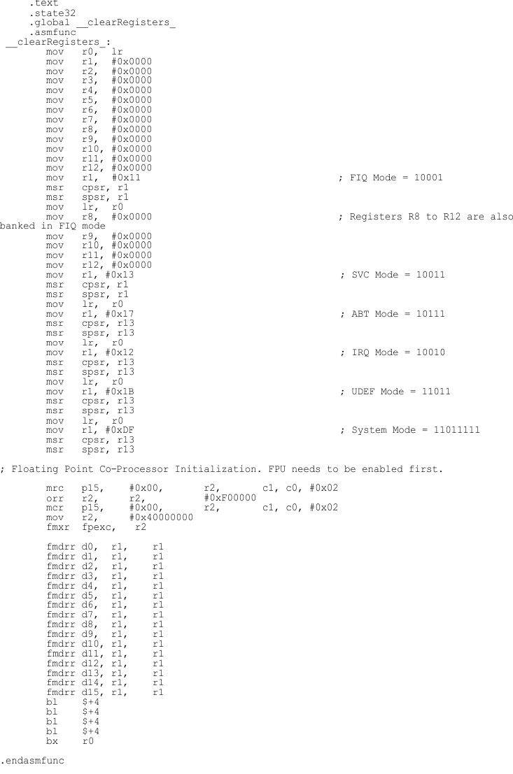
6.5.4.3 CPU Registers Initialization
To avoid an erroneous CCM-R5F compare error, the application software must ensure that the CPU registers of both CPUs are initialized with the same values before the registers are used, including function calls where the register values are pushed onto the stack.
Example routine for CPU register initialization:
6.5.5 CPU Self-Test
The CPU STC (Self-Test Controller) is used to test the two Cortex-R5F CPU Cores using the Deterministic Logic BIST Controller as the test engine.
The main features of the self-test controller are:
- Ability to divide the complete test run into independent test intervals
- Capable of running the complete test as well as running few intervals at a time
- Ability to continue from the last executed interval (test set) as well as ability to restart from the beginning (First test set)
- Complete isolation of the self-tested CPU core from rest of the system during the self-test run
- Ability to capture the Failure interval number
- Time-out counter for the CPU self-test run as a fail-safe feature
6.5.5.1 Application Sequence for CPU Self-Test
- Configure clock domain frequencies.
- Select number of test intervals to be run.
- Configure the time-out period for the self-test run.
- Enable self-test.
- Wait for CPU reset.
- In the reset handler, read CPU self-test status to identify any failures.
- Retrieve CPU state if required.
For more information see the device technical reference manual.
6.5.5.2 CPU Self-Test Clock Configuration
The maximum clock rate for the self-test is 110 MHz. The STCCLK is divided down from the CPU clock. This divider is configured by the STCCLKDIV register at address 0xFFFFE644.
For more information see the device-specific Technical Reference Manual.
6.5.5.3 CPU Self-Test Coverage
The self-test, if enabled, is automatically applied to the entire processor group. Self-test will only start when nCLKSTOPPEDm is asserted which indicates the CPU cores and the ACP interface are in quiescent state. While the processor group is in self-test, other masters can still function normally including accesses to the system memory such as the L2 SRAM. Because uSCU is part of the processor group under self-test, the cache coherency checking will be bypassed.
When the self-test is completed, reset is asserted to all logic subjected to self-test. After self-test is complete, software must invalidate the cache accordingly.
The default value of the CPU LBIST clock prescaler is’ divide-by-1’. A prescalar in the STC module can be used to configure the CPU LBIST frequency with respect to the CPU GCLK frequency.
Table 6-9 lists the CPU test coverage achieved for each self-test interval. It also lists the cumulative test cycles. The test time can be calculated by multiplying the number of test cycles with the STC clock period.
Table 6-9 CPU Self-Test Coverage
| INTERVALS | TEST COVERAGE, % | TEST CYCLES |
|---|---|---|
| 0 | 0 | 0 |
| 1 | 56.85 | 1629 |
| 2 | 64.19 | 3258 |
| 3 | 68.76 | 4887 |
| 4 | 71.99 | 6516 |
| 5 | 75 | 8145 |
| 6 | 76.61 | 9774 |
| 7 | 78.08 | 11403 |
| 8 | 79.2 | 13032 |
| 9 | 80.18 | 14661 |
| 10 | 81.03 | 16290 |
| 11 | 81.9 | 17919 |
| 12 | 82.58 | 19548 |
| 13 | 83.24 | 21177 |
| 14 | 83.73 | 22806 |
| 15 | 84.15 | 24435 |
| 16 | 84.52 | 26064 |
| 17 | 84.9 | 27693 |
| 18 | 85.26 | 29322 |
| 19 | 85.68 | 30951 |
| 20 | 86.05 | 32580 |
| 21 | 86.4 | 34209 |
| 22 | 86.68 | 35838 |
| 23 | 86.94 | 37467 |
| 24 | 87.21 | 39096 |
| 25 | 87.48 | 40725 |
| 26 | 87.74 | 42354 |
| 27 | 87.98 | 43983 |
| 28 | 88.18 | 45612 |
| 29 | 88.38 | 47241 |
| 30 | 88.56 | 48870 |
| 31 | 88.75 | 50499 |
| 32 | 88.93 | 52128 |
| 33 | 89.1 | 53757 |
| 34 | 89.23 | 55386 |
| 35 | 89.41 | 57015 |
| 36 | 89.55 | 58644 |
| 37 | 89.7 | 60273 |
| 38 | 89.83 | 61902 |
| 39 | 89.96 | 63531 |
| 40 | 90.1 | 65160 |
6.5.6 N2HET STC / LBIST Self-Test Coverage
Logic BIST self-test capability for N2HETs is available in this device. The STC2 can be configured to perform self-test for both N2HETs at the same time or one at the time. The default value of the N2HET LBIST clock prescaler is divide-by-1. However, the maximum clock rate for the N2HET STC / LBIST is VCLK/2. N2HET STC test should not be executed concurrently with CPU STC test.
Table 6-10 N2HET Self-Test Coverage
| INTERVALS | TEST COVERAGE, % | TEST CYCLES |
|---|---|---|
| 0 | 0 | 0 |
| 1 | 70.01 | 1365 |
| 2 | 77.89 | 2730 |
| 3 | 81.73 | 4095 |
| 4 | 84.11 | 5460 |
| 5 | 86.05 | 6825 |
| 6 | 87.78 | 8190 |
| 7 | 88.96 | 9555 |
| 8 | 89.95 | 10920 |
| 9 | 90.63 | 12285 |
6.6 Clocks
6.6.1 Clock Sources
Table 6-11 lists the available clock sources on the device. Each clock source can be enabled or disabled using the CSDISx registers in the system module. The clock source number in the table corresponds to the control bit in the CSDISx register for that clock source.
Table 6-11 also lists the default state of each clock source.
Table 6-11 Available Clock Sources
| CLOCK SOURCE NO. |
NAME | DESCRIPTION | DEFAULT STATE |
|---|---|---|---|
| 0 | OSCIN | Main Oscillator | Enabled |
| 1 | PLL1 | Output From PLL1 | Disabled |
| 2 | Reserved | Reserved | Disabled |
| 3 | EXTCLKIN1 | External Clock Input 1 | Disabled |
| 4 | CLK80K | Low-Frequency Output of Internal Reference Oscillator | Enabled |
| 5 | CLK10M | High-Frequency Output of Internal Reference Oscillator | Enabled |
| 6 | PLL2 | Output From PLL2 | Disabled |
| 7 | EXTCLKIN2 | External Clock Input 2 | Disabled |
6.6.1.1 Main Oscillator
The oscillator is enabled by connecting the appropriate fundamental resonator/crystal and load capacitors across the external OSCIN and OSCOUT pins as shown in Figure 6-3. The oscillator is a single-stage inverter held in bias by an integrated bias resistor. This resistor is disabled during leakage test measurement and low power modes.
NOTE
TI strongly encourages each customer to submit samples of the device to the resonator/crystal vendors for validation. The vendors are equipped to determine which load capacitors will best tune their resonator/crystal to the microcontroller device for optimum start-up and operation over temperature and voltage extremes.
An external oscillator source can be used by connecting a 3.3-V clock signal to the OSCIN terminal and leaving the OSCOUT terminal unconnected (open) as shown in Figure 6-3.
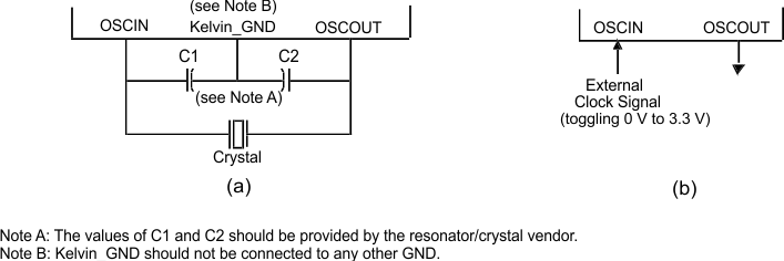 Figure 6-3 Recommended Crystal/Clock Connection
6.6.1.1.1 Timing Requirements for Main Oscillator
Table 6-12 Timing Requirements for Main Oscillator
| MIN | NOM | MAX | UNIT | ||
|---|---|---|---|---|---|
| tc(OSC) | Cycle time, OSCIN (when using a sine-wave input) | 50 | 200 | ns | |
| tc(OSC_SQR) | Cycle time, OSCIN, (when input to the OSCIN is a square wave) | 50 | 200 | ns | |
| tw(OSCIL) | Pulse duration, OSCIN low (when input to the OSCIN is a square wave) | 15 | ns | ||
| tw(OSCIH) | Pulse duration, OSCIN high (when input to the OSCIN is a square wave) | 15 | ns | ||
6.6.1.2 Low-Power Oscillator
The Low-Power Oscillator (LPO) is comprised of two oscillators — HF LPO and LF LPO, in a single macro.
6.6.1.2.1 Features
The main features of the LPO are:
- Supplies a clock at extremely low power to reduce power consumption. This is connected as clock source 4 of the Global Clock Module (GCM).
- Supplies a high-frequency clock for nontiming-critical systems. This is connected as clock source 5 of the GCM.
- Provides a comparison clock for the crystal oscillator failure detection circuit.
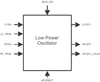 Figure 6-4 LPO Block Diagram
Figure 6-4 shows a block diagram of the internal reference oscillator. This is a low-power oscillator (LPO) and provides two clock sources: one nominally 80 kHz and one nominally 10 MHz.
6.6.1.2.2 LPO Electrical and Timing Specifications
Table 6-13 LPO Specifications
6.6.1.3 Phase-Locked Loop (PLL) Clock Modules
The PLL is used to multiply the input frequency to some higher frequency.
The main features of the PLL are:
- Frequency modulation can be optionally superimposed on the synthesized frequency of PLL1. The frequency modulation capability of PLL2 is permanently disabled.
- Configurable frequency multipliers and dividers
- Built-in PLL Slip monitoring circuit
- Option to reset the device on a PLL slip detection
6.6.1.3.1 Block Diagram
Figure 6-5 shows a high-level block diagram of the two PLL macros on this microcontroller. PLLCTL1 and PLLCTL2 are used to configure the multiplier and dividers for the PLL1. PLLCTL3 is used to configure the multiplier and dividers for PLL2.
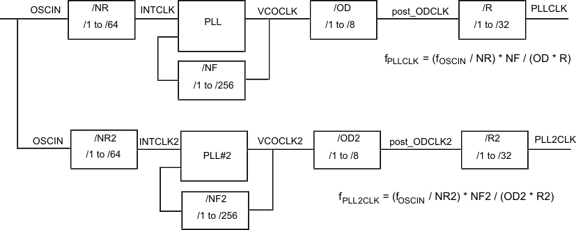 Figure 6-5 ZWT PLLx Block Diagram
6.6.1.3.2 PLL Timing Specifications
Table 6-14 PLL Timing Specifications
| PARAMETER | MIN | MAX | UNIT | |
|---|---|---|---|---|
| fINTCLK | PLL1 Reference Clock frequency | 1 | 20 | MHz |
| fpost_ODCLK | Post-ODCLK – PLL1 Post-divider input clock frequency | 400 | MHz | |
| fVCOCLK | VCOCLK – PLL1 Output Divider (OD) input clock frequency | 550 | MHz | |
| fINTCLK2 | PLL2 Reference Clock frequency | 1 | 20 | MHz |
| fpost_ODCLK2 | Post-ODCLK – PLL2 Post-divider input clock frequency | 400 | MHz | |
| fVCOCLK2 | VCOCLK – PLL2 Output Divider (OD) input clock frequency | 550 | MHz | |
6.6.1.4 External Clock Inputs
The device supports up to two external clock inputs. This clock input must be a square-wave input. Table 6-15 specifies the electrical and timing requirements for these clock inputs.
Table 6-15 External Clock Timing and Electrical Specifications
| PARAMETER | MIN | MAX | UNIT | |
|---|---|---|---|---|
| fEXTCLKx | External clock input frequency | 80 | MHz | |
| tw(EXTCLKIN)H | EXTCLK high-pulse duration | 6 | ns | |
| tw(EXTCLKIN)L | EXTCLK low-pulse duration | 6 | ns | |
| viL(EXTCLKIN) | Low-level input voltage | –0.3 | 0.8 | V |
| viH(EXTCLKIN) | High-level input voltage | 2 | VCCIO + 0.3 | V |
6.6.2 Clock Domains
6.6.2.1 Clock Domain Descriptions
Table 6-16 lists the device clock domains and their default clock sources. Table 6-16 also lists the system module control register that is used to select an available clock source for each clock domain.
Table 6-16 Clock Domain Descriptions
| CLOCK DOMAIN | CLOCK DISABLE BIT | DEFAULT SOURCE |
SOURCE SELECTION REGISTER |
SPECIAL CONSIDERATIONS |
|---|---|---|---|---|
| GCLK1 | SYS.CDDIS.0 | OSCIN | SYS.GHVSRC[3:0] |
|
| GCLK2 | SYS.CDDIS.0 | OSCIN | SYS.GHVSRC[3:0] |
|
| HCLK | SYS.CDDIS.1 | OSCIN | SYS.GHVSRC[3:0] |
|
| VCLK | SYS.CDDIS.2 | OSCIN | SYS.GHVSRC[3:0] |
|
| VCLK2 | SYS.CDDIS.3 | OSCIN | SYS.GHVSRC[3:0] |
|
| VCLK3 | SYS.CDDIS.8 | OSCIN | SYS.GHVSRC[3:0] |
|
| VCLKA1 | SYS.CDDIS.4 | VCLK | SYS.VCLKASRC[3:0] |
|
| VCLKA2 | SYS.CDDIS.5 | VCLK | SYS.VCLKASRC[3:0] |
|
| VCLKA4 | SYS.CDDIS.11 | VCLK | SYS.VCLKACON1[19:16] |
|
| VCLKA4_DIVR | SYS.VCLKACON1.20 | VCLK | SYS.VCLKACON1[19:16] |
|
| RTICLK1 | SYS.CDDIS.6 | VCLK | SYS.RCLKSRC[3:0] |
|
6.6.2.2 Mapping of Clock Domains to Device Modules
Each clock domain has a dedicated functionality as shown in Figure 6-6.
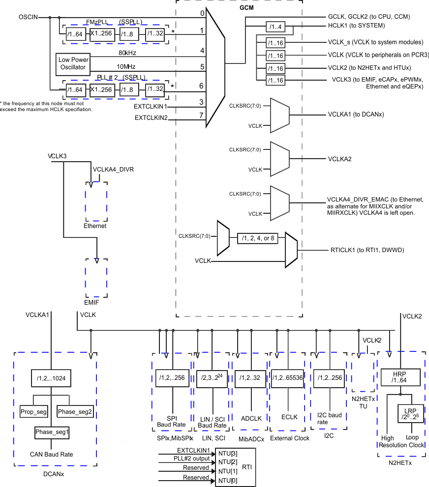 Figure 6-6 Device Clock Domains
6.6.3 Special Clock Source Selection Scheme for VCLKA4_DIVR_EMAC
The MII interface requires VCLKA4_DIVR_EMAC to be 25 MHz and the RMII requires VCLKA4_DIVR_EAMC to be 50 MHz.
These different frequencies are supported by adding special dedicated clock source selection options for the VCLKA4_DIVR_EMAC clock domain. This logic is shown in Figure 6-7.
 Figure 6-7 VCLKA4_DIVR Source Selection Options
The PLL2 post_ODCLK is brought out as a separate output from the PLL wrapper module. There are two additional dividers implemented at the device-level to divide this PLL2 post_ODCLK by 8 and by 16.
As shown in Figure 6-7, the VCLKA4_SRC configured through the system module VCLKACON1 control register is used to determine the clock source for the VCLKA4 and VCLKA4_DIVR. An additional multiplexor is implemented to select between the VCLKA4_DIVR and the two additional clock sources – PLL2 post_ODCLK/8 and post_ODCLK/16.
Table 6-17 lists the VCLKA4_DIVR_EMAC clock source selections.
Table 6-17 VCLKA4_DIVR_EMAC Clock Source Selection
| VCLKA4_SRC FROM VCLKACON1[19–16] | CLOCK SOURCE FOR VCLKA4_DIVR_EMAC |
|---|---|
| 0x0 | OSCIN / VCLKA4R |
| 0x1 | PLL1CLK / VCLKA4R |
| 0x2 | Reserved |
| 0x3 | EXTCLKIN1 / VCLKA4R |
| 0x4 | LF LPO / VCLKA4R |
| 0x5 | HF LPO / VCLKA4R |
| 0x6 | PLL2CLK / VCLKA4R |
| 0x7 | EXTCLKIN2 / VCLKA4R |
| 0x8–0xD | VCLK |
| 0xE | PLL2 post_ODCLK/8 |
| 0xF | PLL2 post_ODCLK/16 |
6.6.4 Clock Test Mode
The RM57Lx platform architecture defines a special mode that allows various clock signals to be selected and output on the ECLK1 terminal and N2HET1[12] device outputs. This special mode, Clock Test Mode, is very useful for debugging purposes and can be configured through the CLKTEST register in the system module. See Table 6-18 and Table 6-19 for the CLKTEST bits value and signal selection.
Table 6-18 Clock Test Mode Options for Signals on ECLK1
Table 6-19 Clock Test Mode Options for Signals on N2HET1[12]
6.7 Clock Monitoring
The LPO Clock Detect (LPOCLKDET) module consists of a clock monitor (CLKDET) and an internal LPO.
The LPO provides two different clock sources – a low frequency (CLK80K) and a high frequency (CLK10M).
The CLKDET is a supervisor circuit for an externally supplied clock signal (OSCIN). In case the OSCIN frequency falls out of a frequency window, the CLKDET flags this condition in the global status register (GLBSTAT bit 0: OSC FAIL) and switches all clock domains sourced by OSCIN to the CLK10M clock (limp mode clock).
The valid OSCIN frequency range is defined as: fCLK10M / 4 < fOSCIN < fCLK10M * 4.
6.7.1 Clock Monitor Timings
 Figure 6-8 LPO and Clock Detection, Untrimmed CLK10M
6.7.2 External Clock (ECLK) Output Functionality
The ECLK1/ECLK2 terminal can be configured to output a prescaled clock signal indicative of an internal device clock. This output can be externally monitored as a safety diagnostic.
6.7.3 Dual Clock Comparators
The Dual Clock Comparator (DCC) module determines the accuracy of selectable clock sources by counting the pulses of two independent clock sources (counter 0 and counter 1). If one clock is out of spec, an error signal is generated. For example, the DCC1 can be configured to use CLK10M as the reference clock (for counter 0) and VCLK as the "clock under test" (for counter 1). This configuration allows the DCC1 to monitor the PLL output clock when VCLK is using the PLL output as its source.
An additional use of this module is to measure the frequency of a selectable clock source. For example, the reference clock is connected to Counter 0 and the signal to be measured is connected to Counter 1. Counter 0 is programmed with a start value of known time duration (measurement time) from the reference clock. Counter 1 is programmed with a maximum start value. Start both counter simultaneously. When Counter 0 decrements to zero, both counter will stop and an error signal is generated if Counter 1 does not reach zero. The frequency of the input signals can be calculated from the count value of Counter 1 and the measurement time.
6.7.3.1 Features
- Takes two different clock sources as input to two independent counter blocks.
- One of the clock sources is the known-good, or reference clock; the second clock source is the "clock under test."
- Each counter block is programmable with initial, or seed values.
- The counter blocks start counting down from their seed values at the same time; a mismatch from the expected frequency for the clock under test generates an error signal which is used to interrupt the CPU.
6.7.3.2 Mapping of DCC Clock Source Inputs
Table 6-20 DCC1 Counter 0 Clock Sources
| CLOCK SOURCE[3:0] | CLOCK NAME |
|---|---|
| Others | Oscillator (OSCIN) |
| 0x5 | High-frequency LPO |
| 0xA | Test clock (TCK) |
Table 6-21 DCC1 Counter 1 Clock Sources
| KEY[3:0] | CLOCK SOURCE[3:0] | CLOCK NAME |
|---|---|---|
| Others | – | N2HET1[31] |
| 0x0 | Main PLL free-running clock output | |
| 0x1 | PLL #2 free-running clock output | |
| 0x2 | Low-frequency LPO | |
| 0xA | 0x3 | High-frequency LPO |
| 0x4 | Reserved | |
| 0x5 | EXTCLKIN1 | |
| 0x6 | EXTCLKIN2 | |
| 0x7 | Reserved | |
| 0x8 - 0xF | VCLK |
Table 6-22 DCC2 Counter 0 Clock Sources
| CLOCK SOURCE[3:0] | CLOCK NAME |
|---|---|
| Others | Oscillator (OSCIN) |
| 0xA | Test clock (TCK) |
Table 6-23 DCC2 Counter 1 Clock Sources
| KEY[3:0] | CLOCK SOURCE[3:0] | CLOCK NAME |
|---|---|---|
| Others | – | N2HET2[0] |
| 0xA | 0x1 | PLL2_post_ODCLK/8 |
| 0x2 | PLL2_post_ODCLK/16 | |
| 0x3 - 0x7 | Reserved | |
| 0x8 - 0xF | VCLK |
6.8 Glitch Filters
Table 6-24 lists the signals with glitch filters present .
Table 6-24 Glitch Filter Timing Specifications
| TERMINAL | PARAMETER | MIN | MAX | UNIT | |
|---|---|---|---|---|---|
| nPORRST | tf(nPORRST) | Filter time nPORRST terminal; pulses less than MIN will be filtered out, pulses greater than MAX will generate a reset(1) | 475 | 2000 | ns |
| nRST | tf(nRST) | Filter time nRST terminal; pulses less than MIN will be filtered out, pulses greater than MAX will generate a reset | 475 | 2000 | ns |
| TEST | tf(TEST) | Filter time TEST terminal; pulses less than MIN will be filtered out, pulses greater than MAX will pass through | 475 | 2000 | ns |
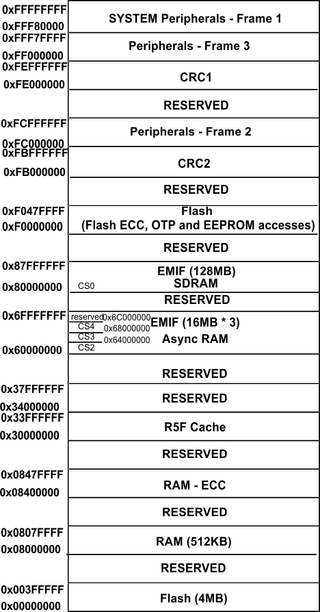
6.9 Device Memory Map
6.9.2 Memory Map Table
Table 6-25 Module Registers / Memories Memory Map
| TARGET NAME | MEMORY SELECT |
ADDRESS RANGE | FRAME SIZE |
ACTUAL SIZE |
RESPONSE FOR ACCESS TO UNIMPLEMENTED LOCATIONS IN FRAME |
|
|---|---|---|---|---|---|---|
| START | END | |||||
| Level 2 Memories | ||||||
| Level 2 Flash Data Space | 0x0000_0000 | 0x003F_FFFF | 4MB | 4MB | Abort | |
| Level 2 RAM | 0x0800_0000 | 0x083F_FFFF | 4MB | 512KB | Abort | |
| Level 2 RAM ECC | 0x0840_0000 | 0x087F_FFFF | 4MB | 512KB | ||
| Accelerator Coherency Port | ||||||
| Accelerator Coherency Port | 0x0800_0000 | 0x087F_FFFF | 8MB | 512KB | Abort | |
| Level 1 Cache Memories | ||||||
| Cortex-R5F Data Cache Memory | 0x3000_0000 | 0x30FF_FFFF | 16MB | 32KB | Abort | |
| Cortex-R5F Instruction Cache Memory | 0x3100_0000 | 0x31FF_FFFF | 16MB | 32KB | ||
| External Memory Accesses | ||||||
| EMIF Chip Select 2 (asynchronous) | 0x6000_0000 | 0x63FF_FFFF | 64MB | 16MB | Access to "Reserved" space will generate Abort | |
| EMIF Chip Select 3 (asynchronous) | 0x6400_0000 | 0x67FF_FFFF | 64MB | 16MB | ||
| EMIF Chip Select 4 (asynchronous) | 0x6800_0000 | 0x6BFF_FFFF | 64MB | 16MB | ||
| EMIF Chip Select 0 (synchronous) | 0x8000_0000 | 0x87FF_FFFF | 128MB | 128MB | ||
| Flash OTP, ECC, EEPROM Bank | ||||||
| Customer OTP, Bank0 | 0xF000_0000 | 0xF000_1FFF | 8KB | 4KB | Abort | |
| Customer OTP, Bank1 | 0xF000_2000 | 0xF000_3FFF | 8KB | 4KB | ||
| Customer OTP, EEPROM Bank | 0xF000_E000 | 0xF000_FFFF | 8KB | 1KB | ||
| Customer OTP-ECC, Bank0 | 0xF004_0000 | 0xF004_03FF | 1KB | 512B | ||
| Customer OTP-ECC, Bank1 | 0xF004_0400 | 0xF004_07FF | 1KB | 512B | ||
| Customer OTP-ECC, EEPROM Bank | 0xF004_1C00 | 0xF004_1FFF | 1KB | 128B | ||
| TI OTP, Bank0 | 0xF008_0000 | 0xF008_1FFF | 8KB | 4KB | ||
| TI OTP, Bank1 | 0xF008_2000 | 0xF008_3FFF | 8KB | 4KB | ||
| TI OTP, EEPROM Bank | 0xF008_E000 | 0xF008_FFFF | 8KB | 1KB | ||
| TI OTP-ECC, Bank0 | 0xF00C_0000 | 0xF00C_03FF | 1KB | 512B | ||
| TI OTP-ECC, Bank1 | 0xF00C_0400 | 0xF00C_07FF | 1KB | 512B | Abort | |
| TI OTP-ECC, EEPROM Bank | 0xF00C_1C00 | 0xF00C_1FFF | 1KB | 128B | ||
| EEPROM Bank-ECC | 0xF010_0000 | 0xF01F_FFFF | 1MB | 16KB | ||
| EEPROM Bank | 0xF020_0000 | 0xF03F_FFFF | 2MB | 128KB | ||
| Flash Data Space ECC | 0xF040_0000 | 0xF05F_FFFF | 2MB | 512KB | ||
| Interconnect SDC MMR | ||||||
| Interconnect SDC MMR | 0xFA00_0000 | 0xFAFF_FFFF | 16MB | 16MB | ||
| Registers/Memories under PCR2 (Peripheral Segment 2) | ||||||
| CPPI Memory Slave (Ethernet RAM) | PCS[41] | 0xFC52_0000 | 0xFC52_1FFF | 8KB | 8KB | Abort |
| CPGMAC Slave (Ethernet Slave) | PS[30]-PS[31] | 0xFCF7_8000 | 0xFCF7_87FF | 2KB | 2KB | No Error |
| CPGMACSS Wrapper (Ethernet Wrapper) | PS[29] | 0xFCF7_8800 | 0xFCF7_88FF | 256B | 256B | No Error |
| Ethernet MDIO Interface | PS[29] | 0xFCF7_8900 | 0xFCF7_89FF | 256B | 256B | No Error |
| ePWM1 | PS[28] | 0xFCF7_8C00 | 0xFCF7_8CFF | 256B | 256B | Abort |
| ePWM2 | 0xFCF7_8D00 | 0xFCF7_8DFF | 256B | 256B | Abort | |
| ePWM3 | 0xFCF7_8E00 | 0xFCF7_8EFF | 256B | 256B | Abort | |
| ePWM4 | 0xFCF7_8F00 | 0xFCF7_8FFF | 256B | 256B | Abort | |
| ePWM5 | PS[27] | 0xFCF7_9000 | 0xFCF7_90FF | 256B | 256B | Abort |
| ePWM6 | 0xFCF7_9100 | 0xFCF7_91FF | 256B | 256B | Abort | |
| ePWM7 | 0xFCF7_9200 | 0xFCF7_92FF | 256B | 256B | Abort | |
| eCAP1 | 0xFCF7_9300 | 0xFCF7_93FF | 256B | 256B | Abort | |
| eCAP2 | PS[26] | 0xFCF7_9400 | 0xFCF7_94FF | 256B | 256B | Abort |
| eCAP3 | 0xFCF7_9500 | 0xFCF7_95FF | 256B | 256B | Abort | |
| eCAP4 | 0xFCF7_9600 | 0xFCF7_96FF | 256B | 256B | Abort | |
| eCAP5 | 0xFCF7_9700 | 0xFCF7_97FF | 256B | 256B | Abort | |
| eCAP6 | PS[25] | 0xFCF7_9800 | 0xFCF7_98FF | 256B | 256B | Abort |
| eQEP1 | 0xFCF7_9900 | 0xFCF7_99FF | 256B | 256B | Abort | |
| eQEP2 | 0xFCF7_9A00 | 0xFCF7_9AFF | 256B | 256B | Abort | |
| PCR2 registers | PPSE[4]–PPSE[5] | 0xFCFF_1000 | 0xFCFF_17FF | 2KB | 2KB | Reads return zeros, writes have no effect |
| NMPU (EMAC) | PPSE[6] | 0xFCFF_1800 | 0xFCFF_18FF | 512B | 512B | Abort |
| EMIF Registers | PPS[2] | 0xFCFF_E800 | 0xFCFF_E8FF | 256B | 256B | Abort |
| Cyclic Redundancy Checker (CRC) Module Register Frame | ||||||
| CRC1 | 0xFE00_0000 | 0xFEFF_FFFF | 16MB | 512KB | Accesses above 0xFE000200 generate abort. | |
| CRC2 | 0xFB00_0000 | 0xFBFF_FFFF | 16MB | 512KB | Accesses above 0xFB000200 generate abort. | |
| Memories under User PCR3 (Peripheral Segment 3) | ||||||
| MIBSPI5 RAM | PCS[5] | 0xFF0A_0000 | 0xFF0B_FFFF | 128KB | 2KB | Abort for accesses above 2KB |
| MIBSPI4 RAM | PCS[3] | 0xFF06_0000 | 0xFF07_FFFF | 128KB | 2KB | Abort for accesses above 2KB |
| MIBSPI3 RAM | PCS[6] | 0xFF0C_0000 | 0xFF0D_FFFF | 128KB | 2KB | Abort for accesses above 2KB |
| MIBSPI2 RAM | PCS[4] | 0xFF08_0000 | 0xFF09_FFFF | 128KB | 2KB | Abort for accesses above 2KB |
| MIBSPI1 RAM | PCS[7] | 0xFF0E_0000 | 0xFF0F_FFFF | 128KB | 4KB | Abort for accesses above 4KB |
| DCAN4 RAM | PCS[12] | 0xFF18_0000 | 0xFF19_FFFF | 128KB | 8KB | Abort generated for accesses beyond offset 0x2000 |
| DCAN3 RAM | PCS[13] | 0xFF1A_0000 | 0xFF1B_FFFF | 128KB | 8KB | Abort generated for accesses beyond offset 0x2000 |
| DCAN2 RAM | PCS[14] | 0xFF1C_0000 | 0xFF1D_FFFF | 128KB | 8KB | Abort generated for accesses beyond offset 0x2000 |
| DCAN1 RAM | PCS[15] | 0xFF1E_0000 | 0xFF1F_FFFF | 128KB | 8KB | Abort generated for accesses beyond offset 0x2000. |
| MIBADC2 RAM | PCS[29] | 0xFF3A_0000 | 0xFF3B_FFFF | 128KB | 8KB | Wrap around for accesses to unimplemented address offsets lower than 0x1FFF. |
| MIBADC1 RAM | PCS[31] | 0xFF3E_0000 | 0xFF3F_FFFF | 128KB | 8KB | Wrap around for accesses to unimplemented address offsets lower than 0x1FFF. |
| MIBADC1 Look-UP Table | 384 bytes | Look-Up Table for ADC1 wrapper. Starts at address offset 0x2000 and ends at address offset 0x217F. Wrap around for accesses between offsets 0x0180 and 0x3FFF. Abort generation for accesses beyond offset 0x4000. | ||||
| NHET2 RAM | PCS[34] | 0xFF44_0000 | 0xFF45_FFFF | 128KB | 16KB | Wrap around for accesses to unimplemented address offsets lower than 0x3FFF. Abort generated for accesses beyond 0x3FFF. |
| NHET1 RAM | PCS[35] | 0xFF46_0000 | 0xFF47_FFFF | 128KB | 16KB | Wrap around for accesses to unimplemented address offsets lower than 0x3FFF. Abort generated for accesses beyond 0x3FFF. |
| HET TU2 RAM | PCS[38] | 0xFF4C_0000 | 0xFF4D_FFFF | 128KB | 1KB | Abort |
| HET TU1 RAM | PCS[39] | 0xFF4E_0000 | 0xFF4F_FFFF | 128KB | 1KB | Abort |
| CoreSight Debug Components | ||||||
| CoreSight Debug ROM | CSCS[0] | 0xFFA0_0000 | 0xFFA0_0FFF | 4KB | 4KB | Reads return zeros, writes have no effect |
| Cortex-R5F Debug | CSCS[1] | 0xFFA0_1000 | 0xFFA0_1FFF | 4KB | 4KB | Reads return zeros, writes have no effect |
| ETM-R5 | CSCS[2] | 0xFFA0_2000 | 0xFFA0_2FFF | 4KB | 4KB | Reads return zeros, writes have no effect |
| CoreSight TPIU | CSCS[3] | 0xFFA0_3000 | 0xFFA0_3FFF | 4KB | 4KB | Reads return zeros, writes have no effect |
| POM | CSCS[4] | 0xFFA0_4000 | 0xFFA0_4FFF | 4KB | 4KB | Reads return zeros, writes have no effect |
| CTI1 | CSCS[7] | 0xFFA0_7000 | 0xFFA0_7FFF | 4KB | 4KB | Reads return zeros, writes have no effect |
| CTI3 | CSCS[9] | 0xFFA0_9000 | 0xFFA0_9FFF | 4KB | 4KB | Reads return zeros, writes have no effect |
| CTI4 | CSCS[10] | 0xFFA0_A000 | 0xFFA0_AFFF | 4KB | 4KB | Reads return zeros, writes have no effect |
| CSTF | CSCS[11] | 0xFFA0_B000 | 0xFFA0_BFFF | 4KB | 4KB | Reads return zeros, writes have no effect |
| Registers under PCR3 (Peripheral Segment 3) | ||||||
| PCR3 registers | PS[31:30] | 0xFFF7_8000 | 0xFFF7_87FF | 2KB | 2KB | Reads return zeros, writes have no effect |
| HTU1 | PS[22] | 0xFFF7_A400 | 0xFFF7_A4FF | 256B | 256B | Abort |
| HTU2 | PS[22] | 0xFFF7_A500 | 0xFFF7_A5FF | 256B | 256B | Abort |
| NHET1 | PS[17] | 0xFFF7_B800 | 0xFFF7_B8FF | 256B | 256B | Reads return zeros, writes have no effect |
| NHET2 | PS[17] | 0xFFF7_B900 | 0xFFF7_B9FF | 256B | 256B | Reads return zeros, writes have no effect |
| GIO | PS[16] | 0xFFF7_BC00 | 0xFFF7_BCFF | 256B | 256B | Reads return zeros, writes have no effect |
| MIBADC1 | PS[15] | 0xFFF7_C000 | 0xFFF7_C1FF | 512B | 512B | Reads return zeros, writes have no effect |
| MIBADC2 | PS[15] | 0xFFF7_C200 | 0xFFF7_C3FF | 512B | 512B | Reads return zeros, writes have no effect |
| I2C1 | PS[10] | 0xFFF7_D400 | 0xFFF7_D4FF | 256B | 256B | Reads return zeros, writes have no effect |
| I2C2 | PS[10] | 0xFFF7_D500 | 0xFFF7_D5FF | 256B | 256B | Reads return zeros, writes have no effect |
| DCAN1 | PS[8] | 0xFFF7_DC00 | 0xFFF7_DDFF | 512B | 512B | Reads return zeros, writes have no effect |
| DCAN2 | PS[8] | 0xFFF7_DE00 | 0xFFF7_DFFF | 512B | 512B | Reads return zeros, writes have no effect |
| DCAN3 | PS[7] | 0xFFF7_E000 | 0xFFF7_E1FF | 512B | 512B | Reads return zeros, writes have no effect |
| DCAN4 | PS[7] | 0xFFF7_E200 | 0xFFF7_E3FF | 512B | 512B | Reads return zeros, writes have no effect |
| LIN1 | PS[6] | 0xFFF7_E400 | 0xFFF7_E4FF | 256B | 256B | Reads return zeros, writes have no effect |
| SCI3 | PS[6] | 0xFFF7_E500 | 0xFFF7_E5FF | 256B | 256B | Reads return zeros, writes have no effect |
| LIN2 | PS[6] | 0xFFF7_E600 | 0xFFF7_E6FF | 256B | 256B | Reads return zeros, writes have no effect |
| SCI4 | PS[6] | 0xFFF7_E700 | 0xFFF7_E7FF | 256B | 256B | Reads return zeros, writes have no effect |
| MibSPI1 | PS[2] | 0xFFF7_F400 | 0xFFF7_F5FF | 512B | 512B | Reads return zeros, writes have no effect |
| MibSPI2 | PS[2] | 0xFFF7_F600 | 0xFFF7_F7FF | 512B | 512B | Reads return zeros, writes have no effect |
| MibSPI3 | PS[1] | 0xFFF7_F800 | 0xFFF7_F9FF | 512B | 512B | Reads return zeros, writes have no effect |
| MibSPI4 | PS[1] | 0xFFF7_FA00 | 0xFFF7_FBFF | 512B | 512B | Reads return zeros, writes have no effect |
| MibSPI5 | PS[0] | 0xFFF7_FC00 | 0xFFF7_FDFF | 512B | 512B | Reads return zeros, writes have no effect |
| System Modules Control Registers and Memories under PCR1 (Peripheral Segment 1) | ||||||
| DMA RAM | PPCS[0] | 0xFFF8_0000 | 0xFFF8_0FFF | 4KB | 4KB | Abort |
| VIM RAM | PPCS[2] | 0xFFF8_2000 | 0xFFF8_2FFF | 4KB | 4KB | Wrap around for accesses to unimplemented address offsets lower than 0x2FFF. |
| RTP RAM | PPCS[3] | 0xFFF8_3000 | 0xFFF8_3FFF | 4KB | 4KB | Abort |
| Flash Wrapper | PPCS[7] | 0xFFF8_7000 | 0xFFF8_7FFF | 4KB | 4KB | Abort |
| eFuse Farm Controller | PPCS[12] | 0xFFF8_C000 | 0xFFF8_CFFF | 4KB | 4KB | Abort |
| Power Domain Control (PMM) | PPSE[0] | 0xFFFF_0000 | 0xFFFF_01FF | 512B | 512B | Abort |
| FMTM Note: This module is only used by TI during test |
PPSE[1] | 0xFFFF_0400 | 0xFFFF_05FF | 512B | 512B | Reads return zeros, writes have no effect |
| STC2 (NHET1/2) | PPSE[2] | 0xFFFF_0800 | 0xFFFF_08FF | 256B | 256B | Reads return zeros, writes have no effect |
| SCM | PPSE[2] | 0xFFFF_0A00 | 0xFFFF_0AFF | 256B | 256B | Abort |
| EPC | PPSE[3] | 0xFFFF_0C00 | 0xFFFF_0FFF | 1KB | 1KB | Abort |
| PCR1 registers | PPSE[4]–PPSE[5] | 0xFFFF_1000 | 0xFFFF_17FF | 2KB | 2KB | Reads return zeros, writes have no effect |
| NMPU (PS_SCR_S) | PPSE[6] | 0xFFFF_1800 | 0xFFFF_19FF | 512B | 512B | Abort |
| NMPU (DMA Port A) | PPSE[6] | 0xFFFF_1A00 | 0xFFFF_1BFF | 512B | 512B | Abort |
| Pin Mux Control (IOMM) | PPSE[7] | 0xFFFF_1C00 | 0xFFFF_1FFF | 2KB | 1KB | Reads return zeros, writes have no effect |
| System Module - Frame 2 (see the TRM SPNU562) | PPS[0] | 0xFFFF_E100 | 0xFFFF_E1FF | 256B | 256B | Reads return zeros, writes have no effect |
| PBIST | PPS[1] | 0xFFFF_E400 | 0xFFFF_E5FF | 512B | 512B | Reads return zeros, writes have no effect |
| STC1 (Cortex-R5F) | PPS[1] | 0xFFFF_E600 | 0xFFFF_E6FF | 256B | 256B | Reads return zeros, writes have no effect |
| DCC1 | PPS[3] | 0xFFFF_EC00 | 0xFFFF_ECFF | 256B | 256B | Reads return zeros, writes have no effect |
| DMA | PPS[4] | 0xFFFF_F000 | 0xFFFF_F3FF | 1KB | 1KB | Abort |
| DCC2 | PPS[5] | 0xFFFF_F400 | 0xFFFF_F4FF | 256B | 256B | Reads return zeros, writes have no effect |
| ESM register | PPS[5] | 0xFFFF_F500 | 0xFFFF_F5FF | 256B | 256B | Reads return zeros, writes have no effect |
| CCM-R5F | PPS[5] | 0xFFFF_F600 | 0xFFFF_F6FF | 256B | 256B | Reads return zeros, writes have no effect |
| DMM | PPS[5] | 0xFFFF_F700 | 0xFFFF_F7FF | 256B | 256B | Reads return zeros, writes have no effect |
| L2RAMW | PPS[6] | 0xFFFF_F900 | 0xFFFF_F9FF | 256B | 256B | Abort |
| RTP | PPS[6] | 0xFFFF_FA00 | 0xFFFF_FAFF | 256B | 256B | Reads return zeros, writes have no effect |
| RTI + DWWD | PPS[7] | 0xFFFF_FC00 | 0xFFFF_FCFF | 256B | 256B | Reads return zeros, writes have no effect |
| VIM | PPS[7] | 0xFFFF_FD00 | 0xFFFF_FEFF | 512B | 512B | Reads return zeros, writes have no effect |
| System Module - Frame 1 (see the TRM SPNU562) | PPS[7] | 0xFFFF_FF00 | 0xFFFF_FFFF | 256B | 256B | Reads return zeros, writes have no effect |
6.9.3 Special Consideration for CPU Access Errors Resulting in Imprecise Aborts
Any CPU write access to a Normal or Device type memory, which generates a fault, will generate an imprecise abort. The imprecise abort exception is disabled by default and must be enabled for the CPU to handle this exception. The imprecise abort handling is enabled by clearing the "A" bit in the CPU program status register (CPSR).
6.9.4 Master/Slave Access Privileges
Table 6-26 and Table 6-27 list the access permissions for each bus master on the device. A bus master is a module that can initiate a read or a write transaction on the device.
Each slave module on either the CPU Interconnect Subsystem or the Peripheral Interconnect Subsystem is listed in Table 6-27. Allowed indicates that the module listed in the MASTERS column can access that slave module.
Table 6-26 Bus Master / Slave Access Matrix for CPU Interconnect Subsystem
| MASTERS | SLAVES ON CPU INTERCONNECT SUBSYSTEM | ||||
|---|---|---|---|---|---|
| L2 Flash OTP, ECC, Bank 7 (EEPROM) | L2 FLASH | L2 SRAM | CACHE MEMORY | EMIF | |
| CPU Read | Allowed | Allowed | Allowed | Allowed | Allowed |
| CPU Write | Not allowed | Not allowed | Allowed | Allowed | Allowed |
| DMA PortA | Allowed | Allowed | Allowed | Not allowed | Allowed |
| POM | Not allowed | Not allowed | Allowed | Not allowed | Allowed |
| PS_SCR_M | Allowed | Allowed | Allowed | Not allowed | Allowed |
| ACP_M | Not allowed | Not Allowed | Allowed | Not allowed | Not allowed |
Table 6-27 Bus Master / Slave Access Matrix for Peripheral Interconnect Subsystem
| MASTER ID TO PCRx | MASTERS | SLAVES ON PERIPHERAL INTERCONNECT SUBSYSTEM | |||
|---|---|---|---|---|---|
| CRC1/CRC2 | Resources Under PCR2 and PCR3 |
Resources Under PCR1 | CPU Interconnect Subsystem SDC MMR Port (see Section 6.9.6) | ||
| 0 | CPU Read | Allowed | Allowed | Allowed | Allowed |
| CPU Write | Allowed | Allowed | Allowed | Allowed | |
| 1 | Reserved | – | – | – | – |
| 2 | DMA PortB | Allowed | Allowed | Allowed | Not allowed |
| 3 | HTU1 | Not allowed | Not allowed | Not allowed | Not allowed |
| 4 | HTU2 | Not allowed | Not allowed | Not allowed | Not allowed |
| 7 | DMM | Allowed | Allowed | Allowed | Allowed |
| 9 | DAP | Allowed | Allowed | Allowed | Allowed |
| 10 | EMAC | Not allowed | Allowed | Not allowed | Not allowed |
6.9.4.1 Special Notes on Accesses to Certain Slaves
By design only the CPU and debugger can have privileged write access to peripherals under the PCR1 segment. The other masters can only read from these registers.
The master-id filtering check is implemented inside each PCR module of each peripheral segment and can be used to block certain masters from write accesses to certain peripherals. An unauthorized master write access detected by the PCR will result in the transaction being discarded and an error being generated to the ESM module.
The device contains dedicated logic to generate a bus error response on any access to a module that is in a power domain that has been turned off.
6.9.5 MasterID to PCRx
The MasterID associated with each master port on the Peripheral Interconnect Subsystem contains a 4-bit value. The MasterID is passed along with the address and control signals to three PCR modules. PCR decodes the address and control signals to select the peripheral. In addition, it decodes this 4-bit MasterID value to perform memory protection. With 4-bit of MasterID, it allows the PCR to distinguish among 16 different masters to allow or disallow access to a given peripheral. Associated with each peripheral a 16-bit MasterID access protection register is defined. Each bit grants or denies the permission of the corresponding binary coded decimal MasterID. For example, if bit 5 of the access permission register is set, it grants MasterID 5 to access the peripheral. If bit 7 is clear, it denies MasterID 7 to access the peripheral. Figure 6-10 shows the MasterID filtering scheme. Table 6-27 lists the MasterID of each master, which can access the PCRx.
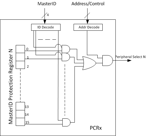 Figure 6-10 PCR MasterID Filtering
6.9.6 CPU Interconnect Subsystem SDC MMR Port
The CPU Interconnect Subsystem SDC MMR Port is a special slave to the Peripheral Interconnect Subsystem. It is memory mapped at starting address of 0xFA00_0000. Various status registers pertaining to the diagnostics of the CPU Interconnect Subsystem can be access through this slave port. The CPU Interconnect Subsystem contains built-in hardware diagnostic checkers which will constantly watch transactions flowing through the interconnect. There is a checker for each master and slave attached to the CPU Interconnect Subsystem. The checker checks the expected behavior against the generated behavior by the interconnect. For example, if the CPU issues a burst read request to the flash, the checker will ensure that the expected behavior is indeed a burst read request to the proper slave module. If the interconnects generates a transaction which is not a read, or not a burst or not to the flash as the destination, then the checker will flag it one of the registers. The detected error will also be signaled to the ESM module. Refer to the Interconnect chapter of the TRM SPNU562 for details on the registers.
Table 6-28 CPU Interconnect Subsystem SDC Register Bit Field Mapping
6.9.7 Parameter Overlay Module (POM) Considerations
The Parameter Overlay Module (POM) is implemented as part of the L2FMC module. It is used to redirect flash memory accesses to external memory interfaces or internal SRAM. The POM has an OCP master port to redirect accesses. The POM MMRs are located in a separate block and read/writes will happen through the Debug APB port on the L2FMC. The POM master port is capable of read accesses only. Inside the CPU Subsystem SCR, the POM master port is connected to both the L2RAMW and EMIF slaves. The primary roles of the POM are:
- The POM snoops the access on the two flash slave ports to determine if access should be remapped or not. It supports 32 regions among the two slave ports.
- If access is to be remapped, then the POM kills the access to the flash bank, and instead redirects the access through its own master.
- Upon obtaining response, the POM populates the response FIFO of the respective port so that the response is delivered back to the original requester.
- The access is unaffected if the request is not mapped to any region, or if the POM is disabled.
- The POM does not add any latency to the flash access when it is turned off.
- The POM does not add any latency to the remapped access (except the latency, if any, associated with the getting the response from the an alternate slave)
6.10 Flash Memory
6.10.1 Flash Memory Configuration
Flash Bank: A separate block of logic consisting of 1 to 16 sectors. Each flash bank normally has a customer-OTP and a TI-OTP area. These flash sectors share input/output buffers, data paths, sense amplifiers, and control logic.
Flash Sector: A contiguous region of flash memory which must be erased simultaneously due to physical construction constraints.
Flash Pump: A charge pump which generates all the voltages required for reading, programming, or erasing the flash banks.
Flash Module: Interface circuitry required between the host CPU and the flash banks and pump module.
Table 6-29 Flash Memory Banks and Sectors
| MEMORY ARRAYS (OR BANKS) | SECTOR NO. | SEGMENT | LOW ADDRESS | HIGH ADDRESS |
|---|---|---|---|---|
| BANK0 (2.0MB) | 0 | 16KB | 0x0000_0000 | 0x0000_3FFF |
| 1 | 16KB | 0x0000_4000 | 0x0000_7FFF | |
| 2 | 16KB | 0x0000_8000 | 0x0000_BFFF | |
| 3 | 16KB | 0x0000_C000 | 0x0000_FFFF | |
| 4 | 16KB | 0x0001_0000 | 0x0001_3FFF | |
| 5 | 16KB | 0x0001_4000 | 0x0001_7FFF | |
| 6 | 32KB | 0x0001_8000 | 0x0001_FFFF | |
| 7 | 128KB | 0x0002_0000 | 0x0003_FFFF | |
| 8 | 128KB | 0x0004_0000 | 0x0005_FFFF | |
| 9 | 128KB | 0x0006_0000 | 0x0007_FFFF | |
| 10 | 256KB | 0x0008_0000 | 0x000B_FFFF | |
| 11 | 256KB | 0x000C_0000 | 0x000F_FFFF | |
| 12 | 256KB | 0x0010_0000 | 0x0013_FFFF | |
| 13 | 256KB | 0x0014_0000 | 0x0017_FFFF | |
| 14 | 256KB | 0x0018_0000 | 0x001B_FFFF | |
| 15 | 256KB | 0x001C_0000 | 0x001F_FFFF | |
| BANK1 (2.0MB) | 0 | 128KB | 0x0020_0000 | 0x0021_FFFF |
| 1 | 128KB | 0x0022_0000 | 0x0023_FFFF | |
| 2 | 128KB | 0x0024_0000 | 0x0025_FFFF | |
| 3 | 128KB | 0x0026_0000 | 0x0027_FFFF | |
| 4 | 128KB | 0x0028_0000 | 0x0029_FFFF | |
| 5 | 128KB | 0x002A_0000 | 0x002B_FFFF | |
| 6 | 128KB | 0x002C_0000 | 0x002D_FFFF | |
| 7 | 128KB | 0x002E_0000 | 0x002F_FFFF | |
| 8 | 128KB | 0x0030_0000 | 0x0031_FFFF | |
| 9 | 128KB | 0x0032_0000 | 0x0033_FFFF | |
| 10 | 128KB | 0x0034_0000 | 0x0035_FFFF | |
| 11 | 128KB | 0x0036_0000 | 0x0037_FFFF | |
| 12 | 128KB | 0x0038_0000 | 0x0039_FFFF | |
| 13 | 128KB | 0x003A_0000 | 0x003B_FFFF | |
| 14 | 128KB | 0x003C_0000 | 0x003D_FFFF | |
| 15 | 128KB | 0x003E_0000 | 0x003F_FFFF |
6.10.2 Main Features of Flash Module
- Support for multiple flash banks for program and/or data storage
- Simultaneous read accesses on two banks while performing program or erase operation on any other bank
- Integrated state machines to automate flash erase and program operations
- Software interface for flash program and erase operations
- Pipelined mode operation to improve instruction access interface bandwidth
- Support for Single Error Correction Double Error Detection (SECDED) block inside Cortex-R5F CPU
- Support for a rich set of diagnostic features
6.10.3 ECC Protection for Flash Accesses
All accesses to the L2 program flash memory are protected by SECDED logic embedded inside the CPU. The flash module provides 8 bits of ECC code for 64 bits of instructions or data fetched from the flash memory. The CPU calculates the expected ECC code based on the 64 bits data received and compares it with the ECC code returned by the flash module. A single-bit error is corrected and flagged by the CPU, while a multibit error is only flagged. The CPU signals an ECC error through its Event bus. This signaling mechanism is not enabled by default and must be enabled by setting the 'X' bit of the Performance Monitor Control Register, c9.

NOTE
ECC is permanently enabled in the CPU L2 interface.
6.10.4 Flash Access Speeds
For information on flash memory access speeds and the relevant wait states required, refer to Section 5.6.
6.10.5 Flash Program and Erase Timings
6.10.5.1 Flash Program and Erase Timings for Program Flash
Table 6-31 Timing Requirements for Program Flash
| MIN | NOM | MAX | UNIT | |||
|---|---|---|---|---|---|---|
| tprog(288bits) | Wide Word (288-bits) programming time | 40 | 300 | µs | ||
| tprog(Total) | 4.0MB programming time(1) | –40°C to 105°C | 21.3 | s | ||
| 0°C to 60°C, for first 25 cycles | 5.3 | 10.6 | s | |||
| terase | Sector/Bank erase time | –40°C to 105°C | 0.3 | 4 | s | |
| 0°C to 60°C, for first 25 cycles | 100 | ms | ||||
| twec | Write/erase cycles with 15-year Data Retention requirement | –40°C to 105°C | 1000 | cycles | ||
6.10.5.2 Flash Program and Erase Timings for Data Flash
Table 6-32 Timing Requirements for Data Flash
| MIN | NOM | MAX | UNIT | |||
|---|---|---|---|---|---|---|
| tprog(72bits) | Wide Word (72-bits) programming time | 47 | 300 | µs | ||
| tprog(Total) | EEPROM Emulation (bank 7) 128KB programming time(1) | –40°C to 105°C | 2.6 | s | ||
| 0°C to 60°C, for first 25 cycles | 775 | 1320 | ms | |||
| EEPROM Emulation (bank 7) Sector/Bank erase time terase(bank7) | –40°C to 105°C | 0.2 | 8 | s | ||
| 0°C to 60°C, for first 25 cycles | 14 | 100 | ms | |||
| twec | Write/erase cycles with 15-year Data Retention requirement | –40°C to 105°C | 100000 | cycles | ||
6.11 L2RAMW (Level 2 RAM Interface Module)
L2RAMW is the TMS570 level two RAM wrapper. Major features implemented in this device include:
- Supports 512KB of L2 SRAMs
- One 64-bit OCP interface
- Built-in ECC generation and evaluation logic
- The ECC logic is enabled by default.
- When enabled, automatic ECC correction on write data from masters on any write sizes (8-,16-,32-,or 64-bit)
- Less than 64-bit write forces built in read-modify-write
- When enabled, reads due to read-modify-write go through ECC correction before data merging with the incoming write data
- Redundant address decoding. Same address decode logic block is duplicated and compared to each other
- Data Trace
- Support tracing of both read and write accesses through RTP module
- Auto initialization of memory banks to known values for both data and their corresponding ECC checksum
6.11.1 L2 SRAM Initialization
The entire L2 SRAM can be globally initialized by setting the corresponding bit in SYS.MSINENA register. When initialized, the memory arrays are written with all zeros for the 64-bit data and the corresponding 8-bit ECC checksum. Hardware memory initialization eliminates ECC error when the CPU reads from an un-initialized memory location which can cause an ECC error. For more information, see the device-specific Technical Reference Manual.
6.12 ECC / Parity Protection for Accesses to Peripheral RAMs
Accesses to some peripheral RAMs are protected by either odd/even parity checking or ECC checking. During a read access the parity or ECC is calculated based on the data read from the peripheral RAM and compared with the good parity or ECC value stored in the peripheral RAM for that peripheral. If any word fails the parity or ECC check, the module generates a ECC/parity error signal that is mapped to the Error Signaling Module. The module also captures the peripheral RAM address that caused the parity error.
The parity or ECC protection for peripheral RAMs is not enabled by default and must be enabled by the application. Each individual peripheral contains control registers to enable the parity or ECC protection for accesses to its RAM.
NOTE
For peripherals with parity protection the CPU read access gets the actual data from the peripheral. The application can choose to generate an interrupt whenever a peripheral RAM parity error is detected.
6.13 On-Chip SRAM Initialization and Testing
6.13.1 On-Chip SRAM Self-Test Using PBIST
6.13.1.1 Features
- Extensive instruction set to support various memory test algorithms
- ROM-based algorithms allow application to run TI production-level memory tests
- Independent testing of all on-chip SRAM
6.13.1.2 PBIST RAM Groups
Table 6-33 PBIST RAM Grouping
| MEMORY | RAM GROUP |
TEST CLOCK | RGS | RDS | MEM TYPE |
NO. BANKS |
TEST PATTERN (ALGORITHM) |
|||
|---|---|---|---|---|---|---|---|---|---|---|
| TRIPLE READ SLOW READ |
TRIPLE READ FAST READ |
March 13N(1)
TWO PORT (cycles) |
March 13N(1)
SINGLE PORT (cycles) |
|||||||
| ALGO MASK 0x1 | ALGO MASK 0x2 | ALGO MASK 0x4 | ALGO MASK 0x8 | |||||||
| PBIST_ROM | 1 | GCM_PBIST_ROM | 1 | 1 | ROM | 1 | 24578 | 8194 | ||
| STC1_1_ROM_R5 | 2 | GCM_PBIST_ROM | 14 | 1 | ROM | 1 | 49154 | 16386 | ||
| STC1_2_ROM_R5 | 3 | GCM_PBIST_ROM | 14 | 2 | ROM | 1 | 49154 | 16386 | ||
| STC2_ROM_NHET | 4 | GCM_PBIST_ROM | 15 | 1 | ROM | 1 | 46082 | 15362 | ||
| AWM1 | 5 | GCM_VCLKP | 2 | 1 | 2P | 1 | 4210 | |||
| DCAN1 | 6 | GCM_VCLKP | 3 | 1..6 | 2P | 2 | 25260 | |||
| DCAN2 | 7 | GCM_VCLKP | 4 | 1..6 | 2P | 2 | 25260 | |||
| DMA | 8 | GCM_HCLK | 5 | 1..6 | 2P | 2 | 37740 | |||
| HTU1 | 9 | GCM_VCLK2 | 6 | 1..6 | 2P | 2 | 6540 | |||
| MIBSPI1 | 10 | GCM_VCLKP | 8 | 1..4 | 2P | 2 | 66760 | |||
| MIBSPI2 | 11 | GCM_VCLKP | 9 | 1..4 | 2P | 2 | 33480 | |||
| MIBSPI3 | 12 | GCM_VCLKP | 10 | 1..4 | 2P | 2 | 33480 | |||
| NHET1 | 13 | GCM_VCLK2 | 11 | 1..12 | 2P | 4 | 50520 | |||
| VIM | 14 | GCM_VCLK | 12 | 1..2 | 2P | 1 | 16740 | |||
| Reserved | 15 | - | - | - | - | - | - | |||
| RTP | 16 | GCM_HCLK | 16 | 1..12 | 2P | 4 | 50520 | |||
| ATB(2) | 17 | GCM_GCLK1 | 17 | 1..16 | 2P | 8 | 133920 | |||
| AWM2 | 18 | GCM_VCLKP | 18 | 1 | 2P | 1 | 4210 | |||
| DCAN3 | 19 | GCM_VCLKP | 19 | 1..6 | 2P | 2 | 25260 | |||
| DCAN4 | 20 | GCM_VCLKP | 20 | 1..6 | 2P | 2 | 25260 | |||
| HTU2 | 21 | GCM_VCLK2 | 21 | 1..6 | 2P | 2 | 6540 | |||
| MIBSPI4 | 22 | GCM_VCLKP | 22 | 1..4 | 2P | 2 | 33480 | |||
| MIBSPI5 | 23 | GCM_VCLKP | 23 | 1..4 | 2P | 2 | 33480 | |||
| NHET2 | 24 | GCM_VCLK2 | 24 | 1..12 | 2P | 4 | 50520 | |||
| Reserved | 26 | GCM_VCLKP | 26 | 1..8 | 2P | 4 | 33680 | |||
| CPGMAC_STATE_RXADDR | 27 | GCM_VCLK3 | 27 | 1..3 | 2P | 2 | 6390 | |||
| CPGMAC_STAT_FIFO | 28 | GCM_VCLK3 | 27 | 4..6 | 2P | 3 | 8730 | |||
| L2RAMW | 29 | GCM_HCLK | 7 | 1 | SP | 4 | 532580 | |||
| 6 | SP | 4 | ||||||||
| L2RAMW | 30 | GCM_HCLK | 32 | 1 | SP | 4 | 1597740 | |||
| 6 | SP | 4 | ||||||||
| 11 | SP | 4 | ||||||||
| 16 | SP | 4 | ||||||||
| 21 | SP | 4 | ||||||||
| 26 | SP | 4 | ||||||||
| R5_ICACHE | 31 | GCM_GCLK1 | 40 | 1 | SP | 4 | 166600 | |||
| 6 | SP | 4 | ||||||||
| 11 | SP | 4 | ||||||||
| 16 | SP | 4 | ||||||||
| R5_DCACHE | 32 | GCM_GCLK1 | 41 | 1 | SP | 4 | 299820 | |||
| 6 | SP | 4 | ||||||||
| 11 | SP | 4 | ||||||||
| 16 | SP | 4 | ||||||||
| 21 | SP | 4 | ||||||||
| 26 | SP | 4 | ||||||||
| Reserved | 33 | GCM_GCLK2 | 43 | 1 | SP | 4 | 166600 | |||
| 6 | SP | 4 | ||||||||
| 11 | SP | 4 | ||||||||
| 16 | SP | 4 | ||||||||
| Reserved | 34 | GCM_GCLK2 | 44 | 1 | SP | 4 | 299820 | |||
| 6 | SP | 4 | ||||||||
| 11 | SP | 4 | ||||||||
| 16 | SP | 4 | ||||||||
| 21 | SP | 4 | ||||||||
| 26 | SP | 4 | ||||||||
| Reserved | 35 | GCM_VCLKP | 26 | 9..11 | SP | 3 | 149910 | |||
| CPGMAC_CPPI | 36 | GCM_VCLK3 | 27 | 7 | SP | 1 | 133170 | |||
| R5_DCACHE_Dirty | 37 | GCM_GCLK1 | 42 | 2 | SP | 1 | 16690 | |||
| Reserved | 38 | - | - | - | - | - | - | |||
Several memory testing algorithms are stored in the PBIST ROM. However, TI only recommends the March13N algorithm for application testing of RAM.
The PBIST ROM clock frequency is limited to the maximum frequency of 82.5 MHz.
The PBIST ROM clock is divided down from HCLK. The divider is selected by programming the ROM_DIV field of the Memory Self-Test Global Control Register (MSTGCR) at address 0xFFFFFF58.
6.13.2 On-Chip SRAM Auto Initialization
This microcontroller allows some of the on-chip memories to be initialized through the Memory Hardware Initialization mechanism in the system module. This hardware mechanism allows an application to program the memory arrays with error detection capability to a known state based on their error detection scheme (odd/even parity or ECC).
The MINITGCR register enables the memory initialization sequence, and the MSINENA register selects the memories that are to be initialized.
For more information on these registers, see the device-specific Technical Reference Manual.
The mapping of the different on-chip memories to the specific bits of the MSINENA registers is provided in Table 6-34.
Table 6-34 Memory Initialization(4)(3)
| CONNECTING MODULE | ADDRESS RANGE | SYS.MSINENA Register Bit # | L2RAMW.MEMINT_ENA Register Bit #(1) | |
|---|---|---|---|---|
| BASE ADDRESS | ENDING ADDRESS | |||
| L2 SRAM | 0x08000000 | 0x0800FFFF | 0 | 0 |
| L2 SRAM | 0x08010000 | 0x0801FFFF | 0 | 1 |
| L2 SRAM | 0x08020000 | 0x0802FFFF | 0 | 2 |
| L2 SRAM | 0x08030000 | 0x0803FFFF | 0 | 3 |
| L2 SRAM | 0x08040000 | 0x0804FFFF | 0 | 4 |
| L2 SRAM | 0x08050000 | 0x0805FFFF | 0 | 5 |
| L2 SRAM | 0x08060000 | 0x0806FFFF | 0 | 6 |
| L2 SRAM | 0x08070000 | 0x0807FFFF | 0 | 7 |
| MIBSPI5 RAM(2) | 0xFF0A0000 | 0xFF0BFFFF | 12 | n/a |
| MIBSPI4 RAM(2) | 0xFF060000 | 0xFF07FFFF | 19 | n/a |
| MIBSPI3 RAM(2) | 0xFF0C0000 | 0xFF0DFFFF | 11 | n/a |
| MIBSPI2 RAM(2) | 0xFF080000 | 0xFF09FFFF | 18 | n/a |
| MIBSPI1 RAM(2) | 0xFF0E0000 | 0xFF0FFFFF | 7 | n/a |
| DCAN4 RAM | 0xFF180000 | 0xFF19FFFF | 20 | n/a |
| DCAN3 RAM | 0xFF1A0000 | 0xFF1BFFFF | 10 | n/a |
| DCAN2 RAM | 0xFF1C0000 | 0xFF1DFFFF | 6 | n/a |
| DCAN1 RAM | 0xFF1E0000 | 0xFF1FFFFF | 5 | n/a |
| MIBADC2 RAM | 0xFF3A0000 | 0xFF3BFFFF | 14 | n/a |
| MIBADC1 RAM | 0xFF3E0000 | 0xFF3FFFFF | 8 | n/a |
| NHET2 RAM | 0xFF440000 | 0xFF45FFFF | 15 | n/a |
| NHET1 RAM | 0xFF460000 | 0xFF47FFFF | 3 | n/a |
| HET TU2 RAM | 0xFF4C0000 | 0xFF4DFFFF | 16 | n/a |
| HET TU1 RAM | 0xFF4E0000 | 0xFF4FFFFF | 4 | n/a |
| DMA RAM | 0xFFF80000 | 0xFFF80FFF | 1 | n/a |
| VIM RAM | 0xFFF82000 | 0xFFF82FFF | 2 | n/a |
NOTE
Peripheral memories not listed in the table either do not support auto-initialization or have implemented auto-initialization controlled directly by their respective peripherals.
6.14 External Memory Interface (EMIF)
6.14.1 Features
The EMIF includes many features to enhance the ease and flexibility of connecting to external asynchronous memories or SDRAM devices. The EMIF features includes support for:
- 3 addressable chip select for asynchronous memories of up to 16MB each
- 1 addressable chip select space for SDRAMs up to 128MB
- 8 or 16-bit data bus width
- Programmable cycle timings such as setup, strobe, and hold times as well as turnaround time
- Select strobe mode
- Extended Wait mode
- Data bus parking
NOTE
For a 32-bit access on the 16-bit EMIF interface, the lower 16-bits (the EMIF_BA[1] will be low) will be put out first followed by the upper 16-bits (EMIF_BA[1] will be high).
6.14.2 Electrical and Timing Specifications
6.14.2.1 Read Timing (Asynchronous RAM)
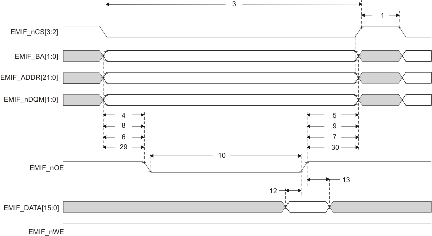 Figure 6-11 Asynchronous Memory Read Timing
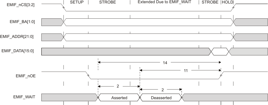 Figure 6-12 EMIFnWAIT Read Timing Requirements
6.14.2.2 Write Timing (Asynchronous RAM)
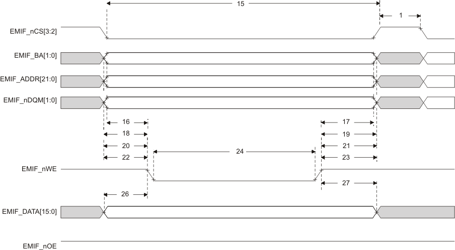 Figure 6-13 Asynchronous Memory Write Timing
 Figure 6-14 EMIFnWAIT Write Timing Requirements
6.14.2.3 EMIF Asynchronous Memory Timing
Table 6-35 EMIF Asynchronous Memory Timing Requirements(1)
| NO. | MIN | NOM | MAX | UNIT | ||
|---|---|---|---|---|---|---|
| Reads and Writes | ||||||
| 2 | tw(EM_WAIT) | Pulse duration, EMIFnWAIT assertion and deassertion | 2E | ns | ||
| Reads | ||||||
| 12 | tsu(EMDV-EMOEH) | Setup time, EMIFDATA[15:0] valid before EMIFnOE high | 11 | ns | ||
| 13 | th(EMOEH-EMDIV) | Hold time, EMIFDATA[15:0] valid after EMIFnOE high | 0.5 | ns | ||
| 14 | tsu(EMOEL-EMWAIT) | Setup Time, EMIFnWAIT asserted before end of Strobe Phase(2) | 4E+14 | ns | ||
| Writes | ||||||
| 28 | tsu(EMWEL-EMWAIT) | Setup Time, EMIFnWAIT asserted before end of Strobe Phase(2) | 4E+14 | ns | ||
Table 6-36 EMIF Asynchronous Memory Switching Characteristics(1)(2)(3)
6.14.2.4 Read Timing (Synchronous RAM)
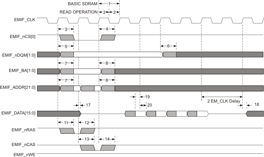 Figure 6-15 Basic SDRAM Read Operation
6.14.2.5 Write Timing (Synchronous RAM)
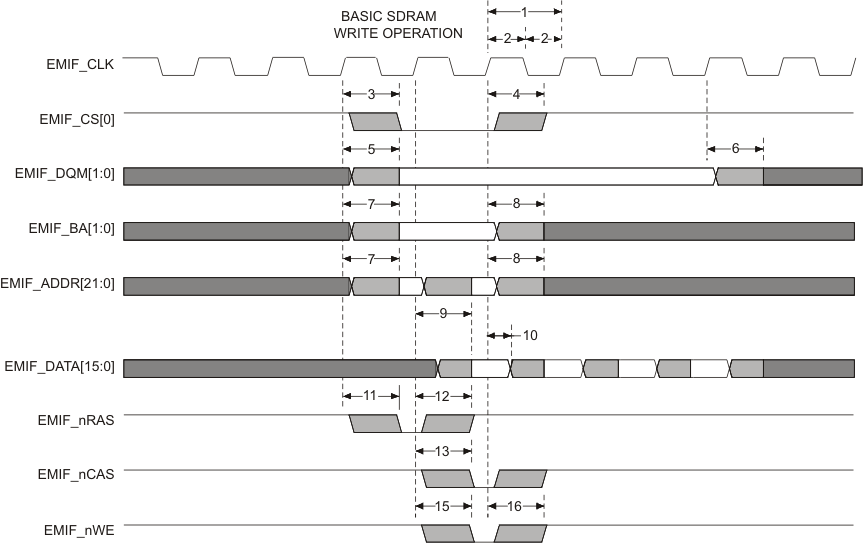 Figure 6-16 Basic SDRAM Write Operation
6.14.2.6 EMIF Synchronous Memory Timing
Table 6-37 EMIF Synchronous Memory Timing Requirements
Table 6-38 EMIF Synchronous Memory Switching Characteristics
| NO. | PARAMETER | MIN | MAX | UNIT | |
|---|---|---|---|---|---|
| 1 | tc(CLK) | Cycle time, EMIF clock EMIF_CLK | 10 | ns | |
| 2 | tw(CLK) | Pulse width, EMIF clock EMIF_CLK high or low | 3 | ns | |
| 3 | td(CLKH-CSV) | Delay time, EMIF_CLK rising to EMIF_nCS[0] valid | 7 | ns | |
| 4 | toh(CLKH-CSIV) | Output hold time, EMIF_CLK rising to EMIF_nCS[0] invalid | 1 | ns | |
| 5 | td(CLKH-DQMV) | Delay time, EMIF_CLK rising to EMIF_nDQM[1:0] valid | 7 | ns | |
| 6 | toh(CLKH-DQMIV) | Output hold time, EMIF_CLK rising to EMIF_nDQM[1:0] invalid | 1 | ns | |
| 7 | td(CLKH-AV) | Delay time, EMIF_CLK rising to EMIF_ADDR[21:0] and EMIF_BA[1:0] valid | 7 | ns | |
| 8 | toh(CLKH-AIV) | Output hold time, EMIF_CLK rising to EMIF_ADDR[21:0] and EMIF_BA[1:0] invalid | 1 | ns | |
| 9 | td(CLKH-DV) | Delay time, EMIF_CLK rising to EMIF_DATA[15:0] valid | 7 | ns | |
| 10 | toh(CLKH-DIV) | Output hold time, EMIF_CLK rising to EMIF_DATA[15:0] invalid | 1 | ns | |
| 11 | td(CLKH-RASV) | Delay time, EMIF_CLK rising to EMIF_nRAS valid | 7 | ns | |
| 12 | toh(CLKH-RASIV) | Output hold time, EMIF_CLK rising to EMIF_nRAS invalid | 1 | ns | |
| 13 | td(CLKH-CASV) | Delay time, EMIF_CLK rising to EMIF_nCAS valid | 7 | ns | |
| 14 | toh(CLKH-CASIV) | Output hold time, EMIF_CLK rising to EMIF_nCAS invalid | 1 | ns | |
| 15 | td(CLKH-WEV) | Delay time, EMIF_CLK rising to EMIF_nWE valid | 7 | ns | |
| 16 | toh(CLKH-WEIV) | Output hold time, EMIF_CLK rising to EMIF_nWE invalid | 1 | ns | |
| 17 | tdis(CLKH-DHZ) | Delay time, EMIF_CLK rising to EMIF_DATA[15:0] tri-stated | 7 | ns | |
| 18 | tena(CLKH-DLZ) | Output hold time, EMIF_CLK rising to EMIF_DATA[15:0] driving | 1 | ns | |
6.15 Vectored Interrupt Manager
There are two on-chip Vector Interrupt Manager (VIM) modules. The VIM module provides hardware assistance for prioritizing and controlling the many interrupt sources present on a device. Interrupts are caused by events outside of the normal flow of program execution. Normally, these events require a timely response from the CPU; therefore, when an interrupt occurs, the CPU switches execution from the normal program flow to an interrupt service routine (ISR).
6.15.1 VIM Features
The VIM module has the following features:
- Supports 128 interrupt channels
- Provides programmable priority for the request lines
- Manages interrupt channels through masking
- Prioritizes interrupt channels to the CPU
- Provides the CPU with the address of the interrupt service routine (ISR) for each interrupt
The two VIM modules are in lockstep. These two VIM modules are memory mapped to the same address space. From a programmer’s model point of view it is only one VIM module. Writes to VIM1 registers and memory will be broadcasted to both VIM1 and VIM2. Reads from VIM1 will only read the VIM1 registers and memory. All interrupt requests which go to the VIM1 module will also go to the VIM2 module. Because the VIM1 and VIM2 have the identical setup, both will result in the same output behavior responding to the same interrupt requests. The second VIM module acts as a diagnostic checker module against the first VIM module. The output signals of the two VIM modules are routed to CCM-R5F module and are compared constantly. Mis-compare detected will be signaled as an error to the ESM module. The lockstep VIM pair takes care of the interrupt generation to the lockstep R5F pair.
6.15.2 Interrupt Generation
To avoid common mode failures the input and output signals of the two VIMs are delayed in a different way as shown in Figure 6-17.
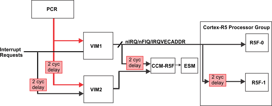 Figure 6-17 Interrupt Generation
6.15.3 Interrupt Request Assignments
Table 6-39 Interrupt Request Assignments
| MODULES | VIM INTERRUPT SOURCES | DEFAULT VIM INTERRUPT CHANNEL |
|---|---|---|
| ESM | ESM high-level interrupt (NMI) | 0 |
| Reserved | Reserved | 1 |
| RTI | RTI1 compare interrupt 0 | 2 |
| RTI | RTI1 compare interrupt 1 | 3 |
| RTI | RTI1 compare interrupt 2 | 4 |
| RTI | RTI1 compare interrupt 3 | 5 |
| RTI | RTI1 overflow interrupt 0 | 6 |
| RTI | RTI1 overflow interrupt 1 | 7 |
| RTI | RTI1 time-base | 8 |
| GIO | GIO high level interrupt | 9 |
| NHET1 | NHET1 high-level interrupt (priority level 1) | 10 |
| HET TU1 | HET TU1 level 0 interrupt | 11 |
| MIBSPI1 | MIBSPI1 level 0 interrupt | 12 |
| LIN1 | LIN1 level 0 interrupt | 13 |
| MIBADC1 | MIBADC1 event group interrupt | 14 |
| MIBADC1 | MIBADC1 software group 1 interrupt | 15 |
| DCAN1 | DCAN1 level 0 interrupt | 16 |
| MIBSPI2 | MIBSPI2 level 0 interrupt | 17 |
| Reserved | Reserved | 18 |
| CRC1 | CRC1 Interrupt | 19 |
| ESM | ESM low-level interrupt | 20 |
| SYSTEM | Software interrupt for Cortex-R5F (SSI) | 21 |
| CPU | Cortex-R5F PMU Interrupt | 22 |
| GIO | GIO low level interrupt | 23 |
| NHET1 | NHET1 low level interrupt (priority level 2) | 24 |
| HET TU1 | HET TU1 level 1 interrupt | 25 |
| MIBSPI1 | MIBSPI1 level 1 interrupt | 26 |
| LIN1 | LIN1 level 1 interrupt | 27 |
| MIBADC1 | MIBADC1 software group 2 interrupt | 28 |
| DCAN1 | DCAN1 level 1 interrupt | 29 |
| MIBSPI2 | MIBSPI2 level 1 interrupt | 30 |
| MIBADC1 | MIBADC1 magnitude compare interrupt | 31 |
| Reserved | Reserved | 32 |
| DMA | FTCA interrupt | 33 |
| DMA | LFSA interrupt | 34 |
| DCAN2 | DCAN2 level 0 interrupt | 35 |
| DMM | DMM level 0 interrupt | 36 |
| MIBSPI3 | MIBSPI3 level 0 interrupt | 37 |
| MIBSPI3 | MIBSPI3 level 1 interrupt | 38 |
| DMA | HBCA interrupt | 39 |
| DMA | BTCA interrupt | 40 |
| EMIF | AEMIFINT | 41 |
| DCAN2 | DCAN2 level 1 interrupt | 42 |
| DMM | DMM level 1 interrupt | 43 |
| DCAN1 | DCAN1 IF3 interrupt | 44 |
| DCAN3 | DCAN3 level 0 interrupt | 45 |
| DCAN2 | DCAN2 IF3 interrupt | 46 |
| FPU | FPU interrupt of Cortex-R5F | 47 |
| Reserved | Reserved | 48 |
| MIBSPI4 | MIBSPI4 level 0 interrupt | 49 |
| MIBADC2 | MibADC2 event group interrupt | 50 |
| MIBADC2 | MibADC2 software group1 interrupt | 51 |
| Reserved | Reserved | 52 |
| MIBSPI5 | MIBSPI5 level 0 interrupt | 53 |
| MIBSPI4 | MIBSPI4 level 1 interrupt | 54 |
| DCAN3 | DCAN3 level 1 interrupt | 55 |
| MIBSPI5 | MIBSPI5 level 1 interrupt | 56 |
| MIBADC2 | MibADC2 software group2 interrupt | 57 |
| Reserved | Reserved | 58 |
| MIBADC2 | MibADC2 magnitude compare interrupt | 59 |
| DCAN3 | DCAN3 IF3 interrupt | 60 |
| L2FMC | FSM_DONE interrupt | 61 |
| Reserved | Reserved | 62 |
| NHET2 | NHET2 level 0 interrupt | 63 |
| SCI3 | SCI3 level 0 interrupt | 64 |
| NHET TU2 | NHET TU2 level 0 interrupt | 65 |
| I2C1 | I2C level 0 interrupt | 66 |
| Reserved | Reserved | 67–72 |
| NHET2 | NHET2 level 1 interrupt | 73 |
| SCI3 | SCI3 level 1 interrupt | 74 |
| NHET TU2 | NHET TU2 level 1 interrupt | 75 |
| Ethernet | C0_MISC_PULSE | 76 |
| Ethernet | C0_TX_PULSE | 77 |
| Ethernet | C0_THRESH_PULSE | 78 |
| Ethernet | C0_RX_PULSE | 79 |
| HWAG1 | HWA_INT_REQ_H | 80 |
| HWAG2 | HWA_INT_REQ_H | 81 |
| DCC1 | DCC1 done interrupt | 82 |
| DCC2 | DCC2 done interrupt | 83 |
| SYSTEM | Reserved | 84 |
| PBIST | PBIST Done | 85 |
| Reserved | Reserved | 86–87 |
| HWAG1 | HWA_INT_REQ_L | 88 |
| HWAG2 | HWA_INT_REQ_L | 89 |
| ePWM1INTn | ePWM1 Interrupt | 90 |
| ePWM1TZINTn | ePWM1 Trip Zone Interrupt | 91 |
| ePWM2INTn | ePWM2 Interrupt | 92 |
| ePWM2TZINTn | ePWM2 Trip Zone Interrupt | 93 |
| ePWM3INTn | ePWM3 Interrupt | 94 |
| ePWM3TZINTn | ePWM3 Trip Zone Interrupt | 95 |
| ePWM4INTn | ePWM4 Interrupt | 96 |
| ePWM4TZINTn | ePWM4 Trip Zone Interrupt | 97 |
| ePWM5INTn | ePWM5 Interrupt | 98 |
| ePWM5TZINTn | ePWM5 Trip Zone Interrupt | 99 |
| ePWM6INTn | ePWM6 Interrupt | 100 |
| ePWM6TZINTn | ePWM6 Trip Zone Interrupt | 101 |
| ePWM7INTn | ePWM7 Interrupt | 102 |
| ePWM7TZINTn | ePWM7 Trip Zone Interrupt | 103 |
| eCAP1INTn | eCAP1 Interrupt | 104 |
| eCAP2INTn | eCAP2 Interrupt | 105 |
| eCAP3INTn | eCAP3 Interrupt | 106 |
| eCAP4INTn | eCAP4 Interrupt | 107 |
| eCAP5INTn | eCAP5 Interrupt | 108 |
| eCAP6INTn | eCAP6 Interrupt | 109 |
| eQEP1INTn | eQEP1 Interrupt | 110 |
| eQEP2INTn | eQEP2 Interrupt | 111 |
| Reserved | Reserved | 112 |
| DCAN4 | DCAN4 Level 0 interrupt | 113 |
| I2C2 | I2C2 interrupt | 114 |
| LIN2 | LIN2 level 0 interrupt | 115 |
| SCI4 | SCI4 level 0 interrupt | 116 |
| DCAN4 | DCAN4 Level 1 interrupt | 117 |
| LIN2 | LIN2 level 1 interrupt | 118 |
| SCI4 | SCI4 level 1 interrupt | 119 |
| DCAN4 | DCAN4 IF3 Interrupt | 120 |
| CRC2 | CRC2 Interrupt | 121 |
| Reserved | Reserved | 122 |
| Reserved | Reserved | 123 |
| EPC | EPC FIFO FULL or CAM FULL interrupt | 124 |
| Reserved | Reserved | 125-127 |
NOTE
Address location 0x00000000 in the VIM RAM is reserved for the phantom interrupt ISR entry; therefore only request channels 0..126 can be used and are offset by one address in the VIM RAM.
NOTE
The EMIF_nWAIT signal has a pull-up on it. The EMIF module generates a "Wait Rise" interrupt whenever it detects a rising edge on the EMIF_nWAIT signal. This interrupt condition is indicated as soon as the device is powered up. This can be ignored if the EMIF_nWAIT signal is not used in the application. If the EMIF_nWAIT signal is actually used in the application, then the external slave memory must always drive the EMIF_nWAIT signal such that an interrupt is not caused due to the default pull-up on this signal.
NOTE
The lower-order interrupt channels are higher priority channels than the higher-order interrupt channels.
NOTE
The application can change the mapping of interrupt sources to the interrupt channels through the interrupt channel control registers (CHANCTRLx) inside the VIM module.
6.16 ECC Error Event Monitoring and Profiling
This device includes an Error Profiling Controller (EPC) module. The main goal of this module is to enable the system to tolerate a certain amount of ECC correctable errors on the same address repeatedly in the memory system with minimal runtime overhead. Main features implemented in this device are described below.
- Capture the address of correctable ECC faults from different sources (for example, CPU, L2RAM, Interconnect) into a 16-entry Content Addressable Memory (CAM).
- For correctable faults, the error handling depends on the below conditions:
- if the incoming address is already in the 16-entry CAM, discard the fail. No error generated to ESM
- if the address is not in the CAM list, and the CAM has empty entries, add the address into the CAM list. In addition, raise the error signal to the ESM group 1 if enabled.
- if the address is not in the CAM list, and the CAM has no empty entries, always raise a signal to the ESM group 1.
- A 4-entry FIFO to store correctable error events and addresses for each IP interface.
- For uncorrectable faults of non-CPU access, capture the address and raise a signal to the ESM group 2.
- The CAM is implemented in memory mapped registers. The CPU can read and write to any entry for diagnostic test as if a real CAM memory macro.
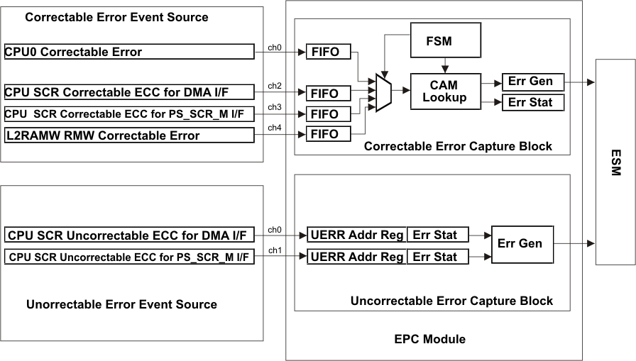 Figure 6-18 EPC Block Diagram
6.16.1 EPC Module Operation
6.16.1.1 Correctable Error Handling
When a correctable error is detected in the system by an IP, it sends the error signal along with the error address to EPC module. The EPC module will scan this error address in the 16-entry CAM. If there is a match then the address is discard and no error is generated to ESM by the ECP. It takes one cycle to scan one address at a time through the CAM. The idea is to allow the system to tolerate a correctable error occurring on the same address because this error has been handled before by the CPU. This error scenario is particularly frequent when the software is in a for loop fetching the same address. Because there are multiple IPs which can simultaneously detect correctable errors in the system, the EPC employs a 4-entry FIFO per IP interface so that error addresses are not lost.
If an address is not matched in the CAM then it depends if there is empty entry in the CAM. If there is an empty entry then the new address is stored into the empty entry. For each entry there is a 4-bit valid key. When a new address is stored the 4-bit key is updated with "1010". It is programmable to generate a correctable error to the ESM if the address is not matched and there is an empty CAM entry. Once CPU is interrupted, it can choose to evaluate the error address and handle it accordingly. The software can also invalidate the entry by writing "0101".
If an dress is not matched and there is no empty entry in the CAM then the correctable error is immediately sent to the ESM. The new error address is lost if there is no empty entry left in the CAM.
6.16.1.2 Uncorrectable Error Handling
Uncorrectable errors reported by the IP (non-CPU access) are immediately captured for their error addresses and update to the uncorrectable error status register. For more information see the device specific technical reference guide SPNU562.
6.17 DMA Controller
The DMA controller is used to transfer data between two locations in the memory map in the background of CPU operations. Typically, the DMA is used to:
- Transfer blocks of data between external and internal data memories
- Restructure portions of internal data memory
- Continually service a peripheral
6.17.1 DMA Features
- 64-bit OCP protocol to perform bus master accesses
- INCR-4 64-bit burst accesses
- Multithreading architecture allowing data of two different channel transfers to be interleaved during nonburst accesses
- 2-port configuration for parallel bus master
- Channels can be assigned to either high-priority queue or low-priority queue. Within each queue, fixed or round-robin priorities can be serviced
- Built-in ECC generation and evaluation logic for internal RAM storing channel transfer information
- Supports multiple interrupt outputs for mapping to multiple interrupt controllers in multicore systems
- 48 requests can be mapped to any 32 channels
- Supports LE endianess
- External ECC Gen/Eval block of DMA support ECC generation for data transactions, and parity for address, and control signals (following Cortex-R5F standard)
- 8 MPU regions
- Channel chaining capability
- Hardware and software DMA requests
- 8-, 16-, 32-, or 64-bit transactions supported
- Multiple addressing modes for source/destination (fixed, increment, offset)
- Auto-initiation
6.17.2 DMA Transfer Port Assignment
There are two ports, port A and port B attached to the DMA controller. When configuring a DMA channel for a transfer, the application must also specify the port associated with the transfer source and destination. Table 6-40 lists the mapping between each port and the resources. For example, if a transfer is to be made from the the flash to the SRAM, the application will need configure the desired DMA channel in the PARx register to select port A as the target for both the source and destination. If a transfer is to be made from the SRAM to a peripheral or a peripheral memory, the application will need to configure the desired DMA channel in the PARx register to select port A for read and port B for write. Likewise, if a transfer is from a peripheral to the SRAM then the PARx will be configured to select port B for read and port A for write.
Table 6-40 DMA Port Assignment
| TARGET NAME | ACCESS PORT OF DMA |
|---|---|
| Flash | Port A |
| SRAM | Port A |
| EMIF | Port A |
| Flash OTP/ECC/EEPROM | Port A |
| All other targets (peripherals, peripheral memories) | Port B |
6.17.3 Default DMA Request Map
The DMA module on this microcontroller has 32 channels and up to 48 hardware DMA requests. The module contains DREQASIx registers which are used to map the DMA requests to the DMA channels. By default, channel 0 is mapped to request 0, channel 1 to request 1, and so on.
Some DMA requests have multiple sources, see Table 6-41. The application must ensure that only one of these DMA request sources is enabled at any time.
Table 6-41 DMA Request Line Connection
| MODULES | DMA REQUEST SOURCES | DMA REQUEST |
|---|---|---|
| MIBSPI1 | MIBSPI1[1](1) | DMAREQ[0] |
| MIBSPI1 | MIBSPI1[0](2) | DMAREQ[1] |
| MIBSPI2 | MIBSPI2[1](1) | DMAREQ[2] |
| MIBSPI2 | MIBSPI2[0](2) | DMAREQ[3] |
| MIBSPI1 / MIBSPI3 / DCAN2 | MIBSPI1[2] / MIBSPI3[2] / DCAN2 IF3 | DMAREQ[4] |
| MIBSPI1 / MIBSPI3 / DCAN2 | MIBSPI1[3] / MIBSPI3[3] / DCAN2 IF2 | DMAREQ[5] |
| DCAN1 / MIBSPI5 | DCAN1 IF2 / MIBSPI5[2] | DMAREQ[6] |
| MIBADC1 / MIBSPI5 | MIBADC1 event / MIBSPI5[3] | DMAREQ[7] |
| MIBSPI1 / MIBSPI3 / DCAN1 | MIBSPI1[4] / MIBSPI3[4] / DCAN1 IF1 | DMAREQ[8] |
| MIBSPI1 / MIBSPI3 / DCAN2 | MIBSPI1[5] / MIBSPI3[5] / DCAN2 IF1 | DMAREQ[9] |
| MIBADC1 / MIBSPI5 | MIBADC1 G1 / MIBSPI5[4] | DMAREQ[10] |
| MIBADC1 / MIBSPI5 | MIBADC1 G2 / MIBSPI5[5] | DMAREQ[11] |
| RTI1 / MIBSPI1 / MIBSPI3 | RTI1 DMAREQ0 / MIBSPI1[6] / MIBSPI3[6] | DMAREQ[12] |
| RTI1 / MIBSPI1 / MIBSPI3 | RTI1 DMAREQ1 / MIBSPI1[7] / MIBSPI3[7] | DMAREQ[13] |
| MIBSPI3 / MibADC2 / MIBSPI5 | MIBSPI3[1](1) / MibADC2 event / MIBSPI5[6] | DMAREQ[14] |
| MIBSPI3 / MIBSPI5 | MIBSPI3[0](2) / MIBSPI5[7] | DMAREQ[15] |
| MIBSPI1 / MIBSPI3 / DCAN1 / MibADC2 | MIBSPI1[8] / MIBSPI3[8] / DCAN1 IF3 / MibADC2 G1 | DMAREQ[16] |
| MIBSPI1 / MIBSPI3 / DCAN3 / MibADC2 | MIBSPI1[9] / MIBSPI3[9] / DCAN3 IF1 / MibADC2 G2 | DMAREQ[17] |
| RTI1 / MIBSPI5 | RTI1 DMAREQ2 / MIBSPI5[8] | DMAREQ[18] |
| RTI1 / MIBSPI5 | RTI1 DMAREQ3 / MIBSPI5[9] | DMAREQ[19] |
| NHET1 / NHET2 / DCAN3 | NHET1 DMAREQ[4] / NHET2 DMAREQ[4] / DCAN3 IF2 | DMAREQ[20] |
| NHET1 / NHET2 / DCAN3 | NHET1 DMAREQ[5] / NHET2 DMAREQ[5] / DCAN3 IF3 | DMAREQ[21] |
| MIBSPI1 / MIBSPI3 / MIBSPI5 | MIBSPI1[10] / MIBSPI3[10] / MIBSPI5[10] | DMAREQ[22] |
| MIBSPI1 / MIBSPI3 / MIBSPI5 | MIBSPI1[11] / MIBSPI3[11] / MIBSPI5[11] | DMAREQ[23] |
| NHET1 / NHET2 / MIBSPI5 | NHET1 DMAREQ[6] / NHET2 DMAREQ[6] / MIBSPI5[12] | DMAREQ[24] |
| NHET1 / NHET2 / MIBSPI5 | NHET1 DMAREQ[7] / NHET2 DMAREQ[7] / MIBSPI5[13] | DMAREQ[25] |
| CRC1 / MIBSPI1 / MIBSPI3 | CRC1 DMAREQ[0] / MIBSPI1[12] / MIBSPI3[12] | DMAREQ[26] |
| CRC1 / MIBSPI1 / MIBSPI3 | CRC1 DMAREQ[1] / MIBSPI1[13] / MIBSPI3[13] | DMAREQ[27] |
| LIN1 / MIBSPI5 | LIN1 receive / MIBSPI5[14] | DMAREQ[28] |
| LIN1 / MIBSPI5 | LIN1 transmit / MIBSPI5[15] | DMAREQ[29] |
| MIBSPI1 / MIBSPI3 / SCI3 / MIBSPI5 | MIBSPI1[14] / MIBSPI3[14] / SCI3 receive / MIBSPI5[1](1) | DMAREQ[30] |
| MIBSPI1 / MIBSPI3 / SCI3 / MIBSPI5 | MIBSPI1[15] / MIBSPI3[15] / SCI3 transmit / MIBSPI5[0](2) | DMAREQ[31] |
| I2C2 / ePWM1 / MIBSPI2 / MIBSPI4 / GIOA | I2C2 receive / ePWM1_SOCA / MIBSPI2[2] / MIBSPI4[2] / GIOA[0] | DMAREQ[32] |
| I2C2 / ePWM 1 / MIBSPI2 / MIBSPI4 / GIOA | I2C2 transmit / ePWM1_SOCB / MIBSPI2[3] / MIBSPI4[3] / GIOA[1] | DMAREQ[33] |
| ePWM2 / MIBSPI2 / MIBSPI4 / GIOA | ePWM2_SOCA / MIBSPI2[4] / MIBSPI4[4] / GIOA[2] | DMAREQ[34] |
| ePWM2 / MIBSPI2 / MIBSPI4 / GIOA | ePWM2_SOCB / MIBSPI2[5] / MIBSPI4[5] / GIOA[3] | DMAREQ[35] |
| ePWM3 / MIBSPI2 / MIBSPI4 / GIOA | ePWM3_SOCA / MIBSPI2[6] / MIBSPI4[6] / GIOA[4] | DMAREQ[36] |
| ePWM3 / MIBSPI2 / MIBSPI4 / GIOA | ePWM3_SOCB / MIBSPI2[7] / MIBSPI4[7] / GIOA[5] | DMAREQ[37] |
| CRC2 / ePWM4 / MIBSPI2 / MIBSPI4 / GIOA | CRC2 DMAREQ[0] / ePWM4_SOCA / MIBSPI2[8] / MIBSPI4[8] / GIOA[6] | DMAREQ[38] |
| CRC2 / ePWM4 / MIBSPI2 / MIBSPI4 / GIOA | CRC2 DMAREQ[1] / ePWM4_SOCB / MIBSPI2[9] / MIBSPI4[9] / GIOA[7] | DMAREQ[39] |
| LIN2 / ePWM5 / MIBSPI2 / MIBSPI4 / GIOB | LIN2 receive / ePWM5_SOCA / MIBSPI2[10] / MIBSPI4[10] / GIOB[0] | DMAREQ[40] |
| LIN2 / ePWM5 / MIBSPI2 / MIBSPI4 / GIOB | LIN2 transmit / ePWM5_SOCB / MIBSPI2[11] / MIBSPI4[11] / GIOB[1] | DMAREQ[41] |
| SCI4 / ePWM6 / MIBSPI2 / MIBSPI4 / GIOB | SCI4 receive / ePWM6_SOCA / MIBSPI2[12] / MIBSPI4[12] / GIOB[2] | DMAREQ[42] |
| SCI4 / ePWM6 / MIBSPI2 / MIBSPI4 / GIOB | SCI4 transmit / ePWM6_SOCB / MIBSPI2[13] / MIBSPI4[13] / GIOB[3] | DMAREQ[43] |
| ePWM7 / MIBSPI2 / MIBSPI4 / GIOB | ePWM7_SOCA / MIBSPI2[14] / MIBSPI4[14] / GIOB[4] | DMAREQ[44] |
| ePWM7 / MIBSPI2 / MIBSPI4 / GIOB / DCAN4 | ePWM7_SOCB / MIBSPI2[15] / MIBSPI4[15] / GIOB[5] / DCAN4 IF1 | DMAREQ[45] |
| GIOB / DCAN4 | GIOB[6] / DCAN4_IF2 | DMAREQ[46] |
| GIOB / DCAN4 | GIOB[7] / DCAN4_IF3 | DMAREQ[47] |
6.17.4 Using a GIO terminal as a DMA Request Input
Each GIO terminal can also directly be used as DMA request input as listed in Table 6-41. The polarity of the GIO terminal to trigger a DMA request can be selected inside the DMA module. To use the GIO terminal as a DMA request input, the corresponding select bit must be set to low. See Figure 6-19 for an illustration. For more information see the technical reference guide SPNU562.
 Figure 6-19 Using a GIO terminal as a DMA Request Input
Table 6-42 GIO DMA Request Disable Mapping
| GIO TERMINAL | GIO DMA REQUEST SELECT BIT |
|---|---|
| GIOA[0] | PINMMR175[0] |
| GIOA[1] | PINMMR175[8] |
| GIOA[2] | PINMMR175[16] |
| GIOA[3] | PINMMR175[24] |
| GIOA[4] | PINMMR176[0] |
| GIOA[5] | PINMMR176[8] |
| GIOA[6] | PINMMR176[16] |
| GIOA[7] | PINMMR176[24] |
| GIOB[0] | PINMMR177[0] |
| GIOB[1] | PINMMR177[8] |
| GIOB[2] | PINMMR177[16] |
| GIOB[3] | PINMMR177[24] |
| GIOB[4] | PINMMR178[0] |
| GIOB[5] | PINMMR178[8] |
| GIOB[6] | PINMMR178[16] |
| GIOB[7] | PINMMR178[24] |
6.18 Real-Time Interrupt Module
The real-time interrupt (RTI) module provides timer functionality for operating systems and for benchmarking code. The RTI module can incorporate several counters that define the time bases needed for scheduling an operating system.
The timers also let you benchmark certain areas of code by reading the values of the counters at the beginning and the end of the desired code range and calculating the difference between the values.
6.18.1 Features
The RTI module has the following features:
- Two independent 64-bit counter blocks
- Four configurable compares for generating operating system ticks or DMA requests. Each event can be driven by either counter block 0 or counter block 1.
- Fast enabling/disabling of events
- Two timestamp (capture) functions for system or peripheral interrupts, one for each counter block
6.18.2 Block Diagrams
Figure 6-20 shows a high-level block diagram for one of the two 64-bit counter blocks inside the RTI module. Both the counter blocks are identical except the Network Time Unit (NTUx) inputs are only available as time-base inputs for the counter block 0. Figure 6-21 shows the compare unit block diagram of the RTI module.
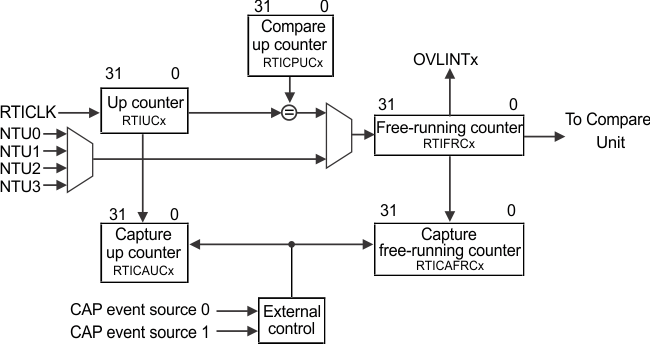 Figure 6-20 Counter Block Diagram
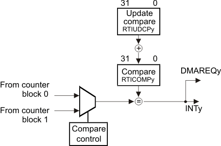 Figure 6-21 Compare Block Diagram
6.18.3 Clock Source Options
The RTI module uses the RTI1CLK clock domain for generating the RTI time bases.
The application can select the clock source for the RTI1CLK by configuring the RCLKSRC register in the system module at address 0xFFFFFF50. The default source for RTI1CLK is VCLK.
For more information on clock sources, see Table 6-11 and Table 6-16.
6.18.4 Network Time Synchronization Inputs
The RTI module supports four Network Time Unit (NTU) inputs that signal internal system events, and which can be used to synchronize the time base used by the RTI module. On this device, these NTU inputs are connected as shown in Table 6-43.
Table 6-43 Network Time Synchronization Inputs
| NTU INPUT | SOURCE |
|---|---|
| 0 | Reserved |
| 1 | Reserved |
| 2 | PLL2 Clock output |
| 3 | EXTCLKIN1 clock input |
6.19 Error Signaling Module
The Error Signaling Module (ESM) manages the various error conditions on the TMS570LCx microcontroller. The error condition is handled based on a fixed severity level assigned to it. Any severe error condition can be configured to drive a low level on a dedicated device terminal called nERROR. The nERROR can be used as an indicator to an external monitor circuit to put the system into a safe state.
6.19.1 ESM Features
The features of the ESM are:
- 160 interrupt/error channels are supported, divided into three groups
- 96 channels with maskable interrupt and configurable error terminal behavior
- 32 error channels with nonmaskable interrupt and predefined error terminal behavior
- 32 channels with predefined error terminal behavior only
- Error terminal to signal severe device failure
- Configurable time base for error signal
- Error forcing capability
6.19.2 ESM Channel Assignments
The ESM integrates all the device error conditions and groups them in the order of severity. Group1 is used for errors of the lowest severity while Group3 is used for errors of the highest severity. The device response to each error is determined by the severity group to which the error is connected. Table 6-45 lists the channel assignment for each group.
Table 6-44 ESM Groups
| ERROR GROUP | INTERRUPT CHARACTERISTICS | INFLUENCE ON ERROR TERMINAL |
|---|---|---|
| Group1 | Maskable, low or high priority | Configurable |
| Group2 | Nonmaskable, high priority | Fixed |
| Group3 | No interrupt generated | Fixed |
Table 6-45 ESM Channel Assignments
6.20 Reset / Abort / Error Sources
Table 6-46 Reset/Abort/Error Sources
| ERROR SOURCE | SYSTEM MODE | ERROR RESPONSE | ESM HOOKUP GROUP.CHANNEL |
|---|---|---|---|
| CPU TRANSACTIONS | |||
| Precise write error (NCNB/Strongly Ordered) | User/Privilege | Precise Abort (CPU) | N/A |
| Precise read error (NCB/Device or Normal) | User/Privilege | Precise Abort (CPU) | N/A |
| Imprecise write error (NCB/Device or Normal) | User/Privilege | Imprecise Abort (CPU) | N/A |
| Illegal instruction | User/Privilege | Undefined Instruction Trap (CPU)(1) | N/A |
| MPU access violation | User/Privilege | Abort (CPU) | N/A |
| Correctable error | User/Privilege | ESM | 1.4 |
| Uncorrectable error | User/Privilege | ESM => NMI | 2.21 |
| LEVEL 2 SRAM | |||
| CPU Write ECC single error (correctable) | User/Privilege | ESM | 1.26 |
| ECC double bit error:
Read-Modify-Write (RMW) ECC double error CPU Write ECC double error |
User/Privilege | Bus Error, ESM => nERROR | 3.3 |
| Uncorrectable error Type A:
Write SECDED malfunction error Redundant address decode error Read SECDED malfunction error |
User/Privilege | Bus Error, ESM => nERROR | 3.14 |
| Uncorrectable error type B:
Memory scrubbing SECDED malfunction error Memory scrubbing Redundant address decode error Memory scrubbing address/control parity error Write data merged mux diagnostic error Write SECDED malfunction diagnostic error Read SECDED malfunction diagnostic error Write ECC correctable and uncorrectable diagnostic error Read ECC correctable and uncorrectable diagnostic error Write data merged mux error Redundant address decode diagnostic error Command parity error on idle |
User/Privilege | ESM => NMI | 2.7 |
| Address/Control parity error | User/Privilege | Bus Error, ESM => nERROR | 3.15 |
| Level 2 RAM illegal address error Memory initialization error | User/Privilege | Bus Error | N/A |
| FLASH | |||
| L2FMC correctable error - single bit ECC error for implicit OTP read | User/Privilege | ESM | 1.6 |
| L2FMC uncorrectable error - double bit ECC error for implicit OTP read | User/Privilege | ESM => NMI | 2.19 |
| L2FMC fatal uncorrectable error:
address parity error/internal parity error address tag error Internal switch time-out |
User/Privilege | Bus Error, ESM => nERROR | 3.13 |
| L2FMC parity error:
Mcmd parity error on Idle command POM idle state parity error Port A/B Idle state parity error |
User/Privilege | ESM => NMI | 2.17 |
| L2FMC nonfatal uncorrectable error:
Response error on POM Response parity error on POM Bank accesses during special operation (program/erase) by the FSM Bank/Pump in sleep Unimplemented special/unavailable space |
User/Privilege | Bus Error | N/A |
| L2FMC register soft error. | User/Privilege | ESM | 1.89 |
| DMA TRANSACTIONS | |||
| Memory access permission violation | User/Privilege | ESM | 1.2 |
| Memory ECC uncorrectable error | User/Privilege | ESM | 1.3 |
| Transaction Error: that is, Bus Parity Error |
User/Privilege | ESM | 1.70 |
| Memory ECC single bit error | User/Privilege | ESM | 1.82 |
| DMA register soft error | User/Privilege | ESM | 1.88 |
| DMA bus error | User/Privilege | ESM | 1.20 |
| EMIF_ECC | |||
| 64-bit Bridge I/F ECC uncorrectable error | User/Privilege | ESM | 1.84 |
| 64-bit Bridge I/F ECC single error | User/Privilege | ESM | 1.85 |
| HET TU1 (HTU1) | |||
| NCNB (Strongly Ordered) transaction with slave error response | User/Privilege | Interrupt => VIM | N/A |
| External imprecise error (Illegal transaction with ok response) | User/Privilege | Interrupt => VIM | N/A |
| Memory access permission violation | User/Privilege | ESM | 1.9 |
| Memory parity error | User/Privilege | ESM | 1.8 |
| HET TU2 (HTU2) | |||
| NCNB (Strongly Ordered) transaction with slave error response | User/Privilege | Interrupt => VIM | N/A |
| External imprecise error (Illegal transaction with ok response) | User/Privilege | Interrupt => VIM | N/A |
| Memory access permission violation | User/Privilege | ESM | 1.9 |
| Memory parity error | User/Privilege | ESM | 1.8 |
| N2HET1 | |||
| Memory parity error | User/Privilege | ESM | 1.7 |
| N2HET2 | |||
| Memory parity error | User/Privilege | ESM | 1.34 |
| MibSPI | |||
| MibSPI1 memory ECC uncorrectable error | User/Privilege | ESM | 1.17 |
| MibSPI2 memory ECC uncorrectable error | User/Privilege | ESM | 1.49 |
| MibSPI3 memory ECC uncorrectable error | User/Privilege | ESM | 1.18 |
| MibSPI4 memory ECC uncorrectable error | User/Privilege | ESM | 1.50 |
| MibSPI5 memory ECC uncorrectable error | User/Privilege | ESM | 1.24 |
| MibSPI1 memory ECC single error | User/Privilege | ESM | 1.77 |
| MibSPI2 memory ECC single error | User/Privilege | ESM | 1.78 |
| MibSPI3 memory ECC single error | User/Privilege | ESM | 1.79 |
| MibSPI4 memory ECC single error | User/Privilege | ESM | 1.80 |
| MibSPI5 memory ECC single error | User/Privilege | ESM | 1.81 |
| MibADC | |||
| MibADC1 Memory parity error | User/Privilege | ESM | 1.19 |
| MibADC2 Memory parity error | User/Privilege | ESM | 1.1 |
| DCAN | |||
| DCAN1 memory ECC uncorrectable error | User/Privilege | ESM | 1.21 |
| DCAN2 memory ECC uncorrectable error | User/Privilege | ESM | 1.23 |
| DCAN3 memory ECC uncorrectable error | User/Privilege | ESM | 1.22 |
| DCAN4 memory ECC uncorrectable error | User/Privilege | ESM | 1.51 |
| DCAN1 memory ECC single error | User/Privilege | ESM | 1.73 |
| DCAN2 memory ECC single error | User/Privilege | ESM | 1.74 |
| DCAN3 memory ECC single error | User/Privilege | ESM | 1.75 |
| DCAN4 memory ECC single error | User/Privilege | ESM | 1.76 |
| PLL | |||
| PLL1 slip error | User/Privilege | ESM | 1.10 |
| PLL2 slip error | User/Privilege | ESM | 1.42 |
| Clock Monitor | |||
| Clock monitor interrupt | User/Privilege | ESM | 1.11 |
| DCC | |||
| DCC1 error | User/Privilege | ESM | 1.30 |
| DCC2 error | User/Privilege | ESM | 1.62 |
| CCM-R5F | |||
| Self-test failure | User/Privilege | ESM | 1.31 |
| CPU Bus Compare failure | User/Privilege | ESM => NMI | 2.2 |
| VIM Bus Compare failure | User/Privilege | ESM => NMI | 2.25 |
| Power Domain Monitor failure | User/Privilege | ESM => NMI | 2.28 |
| CCM-R5F operating status (asserted when not in lockstep or CCM-R5F is in self-test mode) | User/Privilege | ESM | 1.92 |
| EPC (Error Profiling Controller) | |||
| Correctable Error | User/Privilege | ESM | 1.4 |
| Uncorrectable Error | User/Privilege | ESM => NMI | 2.21 |
| SCM (SCR Control module) | |||
| Time-out Error | User/Privilege | ESM | 1.91 |
| Ethernet master interface | |||
| Any error reported by slave being accessed | User/Privilege | ESM | 1.43 |
| VIM | |||
| Memory ECC uncorrectable error | User/Privilege | ESM | 1.15 |
| Memory ECC single bit error | User/Privilege | ESM | 1.83 |
| Voltage Monitor | |||
| VMON out of voltage range | N/A | Reset | N/A |
| Self-Test (LBIST) | |||
| Cortex-R5F CPU self-test (LBIST) error | User/Privilege | ESM | 1.27 |
| NHET Self-test (LBIST) error | User/Privilege | ESM | 1.54 |
| IOMM (terminal multiplexing control) | |||
| Mux configuration error | User/Privilege | ESM | 1.37 |
| Power Domain Control | |||
| Power Domain control access privilege error | User | Imprecise Abort (CPU) | N/A |
| PSCON compare error | User/Privilege | ESM | 1.38 |
| PSCON self-test error | User/Privilege | ESM | 1.39 |
| Efuse farm | |||
| eFuse farm autoload error | User/Privilege | ESM | 3.1 |
| eFuse farm error | User/Privilege | ESM | 1.40 |
| eFuse farm self-test error | User/Privilege | ESM | 1.41 |
| WIndowed Watchdog | |||
| WWD Nonmaskable Interrupt Exception | N/A | ESM | 2.24 |
| Errors Reflected in the SYSESR Register | |||
| Power-Up Reset | N/A | Reset | N/A |
| Oscillator fail / PLL slip(2) | N/A | Reset | N/A |
| Watchdog exception | N/A | Reset | N/A |
| CPUx Reset | N/A | Reset | N/A |
| Software Reset | N/A | Reset | N/A |
| External Reset | N/A | Reset | N/A |
| Register Soft Error | User/Privilege | ESM | 1.90 |
| CPU Interconnect Subsystem | |||
| Diagnostic error | User/Privilege | ESM => Error terminal | 3.12 |
| Global error | User/Privilege | ESM | 1.52 |
| Global Parity error | User/Privilege | ESM | 1.53 |
| NMPU for EMAC | |||
| MPU Access violation error | User/Privilege | ESM | 1.55 |
| NMPU for PS_SCR_S | |||
| MPU Access violation error | User/Privilege | ESM | 1.61 |
| NMPU for DMA Port A | |||
| MPU Access violation error | User/Privilege | ESM | 1.69 |
| PCR1 | |||
| MasterID filtering MPU Access violation error | User/Privilege | Bus Error | N/A |
| PCR2 | |||
| MasterID filtering MPU Access violation error | User/Privilege | Bus Error | N/A |
| PCR3 | |||
| MasterID filtering MPU Access violation error | User/Privilege | Bus Error | N/A |
6.21 Digital Windowed Watchdog
This device includes a Digital Windowed Watchdog (DWWD) module that protects against runaway code execution (see Figure 6-22).
The DWWD module allows the application to configure the time window within which the DWWD module expects the application to service the watchdog. A watchdog violation occurs if the application services the watchdog outside of this window, or fails to service the watchdog at all. The application can choose to generate a system reset or a nonmaskable interrupt to the CPU in case of a watchdog violation.
The watchdog is disabled by default and must be enabled by the application. Once enabled, the watchdog can only be disabled upon a system reset.
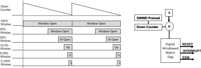 Figure 6-22 Digital Windowed Watchdog Example
6.22 Debug Subsystem
6.22.1 Block Diagram
The device contains an ICEPICK module (version C) to allow JTAG access to the scan chains (see Figure 6-23).
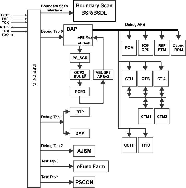 Figure 6-23 Debug Subsystem Block Diagram
6.22.2 Debug Components Memory Map
Table 6-47 Debug Components Memory Map
| MODULE NAME |
FRAME CHIP SELECT |
FRAME ADDRESS RANGE | FRAME SIZE |
ACTUAL SIZE |
RESPONSE FOR ACCESS TO UNIMPLEMENTED LOCATIONS IN FRAME |
|
|---|---|---|---|---|---|---|
| START | END | |||||
| CoreSight Debug ROM | CSCS0 | 0xFFA0_0000 | 0xFFA0_0FFF | 4KB | 4KB | Reads return zeros, writes have no effect |
| Cortex-R5F Debug | CSCS1 | 0xFFA0_1000 | 0xFFA0_1FFF | 4KB | 4KB | Reads return zeros, writes have no effect |
| ETM-R5 | CSCS2 | 0xFFA0_2000 | 0xFFA0_2FFF | 4KB | 4KB | Reads return zeros, writes have no effect |
| CoreSight TPIU | CSCS3 | 0xFFA0_3000 | 0xFFA0_3FFF | 4KB | 4KB | Reads return zeros, writes have no effect |
| POM | CSCS4 | 0xFFA0_4000 | 0xFFA0_4FFF | 4KB | 4KB | Reads return zeros, writes have no effect |
| CTI1 | CSCS7 | 0xFFA0_7000 | 0xFFA0_7FFF | 4KB | 4KB | Reads return zeros, writes have no effect |
| CTI3 | CSCS9 | 0xFFA0_9000 | 0xFFA0_9FFF | 4KB | 4KB | Reads return zeros, writes have no effect |
| CTI4 | CSCS10 | 0xFFA0_A000 | 0xFFA0_AFFF | 4KB | 4KB | Reads return zeros, writes have no effect |
| CSTF | CSCS11 | 0xFFA0_B000 | 0xFFA0_BFFF | 4KB | 4KB | Reads return zeros, writes have no effect |
6.22.3 Embedded Cross Trigger
The Embedded Cross Trigger (ECT) is a modular component that supports the interaction and synchronization of multiple triggering events within a SoC.
The ECT consists of two modules:
- A (Cross Trigger Interface) CTI. The CTI provides the interface between a component or subsystem and the Cross Trigger Matrix (CTM).
- A CTM. The CTM combines the trigger requests generated from CTIs and broadcasts them to all CTIs as channel triggers. This enables subsystems to interact, cross trigger, with one another.
 Figure 6-24 CTI/CTM Integration
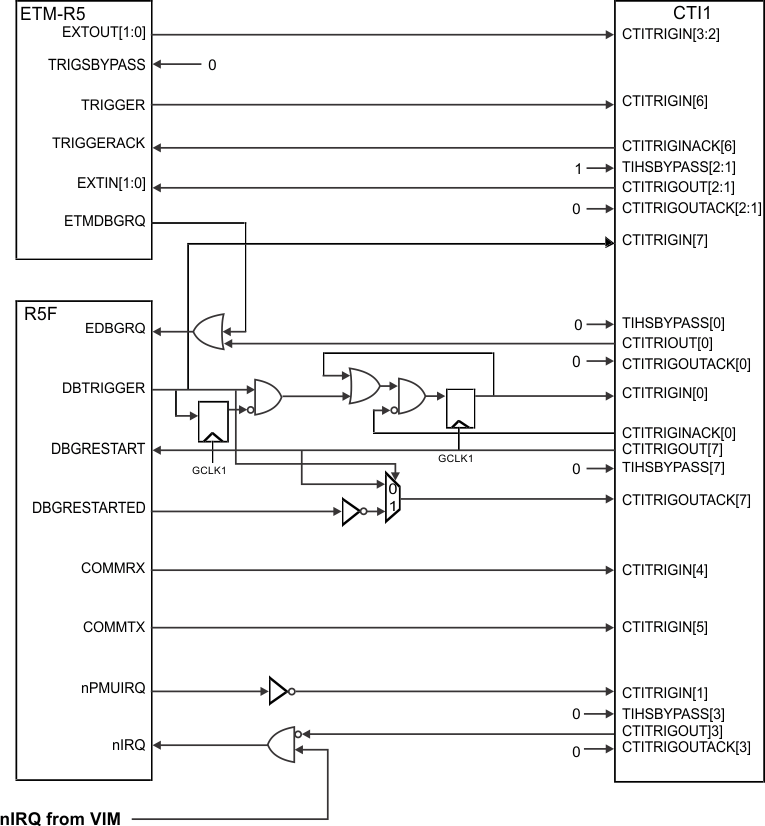 Figure 6-25 CTI1 Mapping
NOTE
ETM-R5, Cortex-R5F and CTI1 run at same frequency.
Table 6-48 CTI1 Mapping
| CTI TRIGGER | Module Signal |
|---|---|
| Trigger Input 0 | From Cortex-R5F DBTRIGGER |
| Trigger Input 1 | From Cortex-R5F nPMUIRQ |
| Trigger Input 2 | From ETM-R5 EXTOUT[0] |
| Trigger Input 3 | From ETM-R5 EXTOUT[1] |
| Trigger Input 4 | From Cortex-R5F COMMRX |
| Trigger Input 5 | From Cortex-R5F COMMTX |
| Trigger Input 6 | From ETM-R5 TRIGGER |
| Trigger Input 7 | From Cortex-R5F DBTRIGGER |
| Trigger Output 0 | To Cortex-R5F EDBGRQ |
| Trigger Output 1 | To ETM-R5 EXTIN[0] |
| Trigger Output 2 | To ETM-R5 EXTIN[1] |
| Trigger Output 3 | To Cortex-R5F nIRQ |
| Trigger Output 4 | Reserved |
| Trigger Output 5 | Reserved |
| Trigger Output 6 | Reserved |
| Trigger Output 7 | To Cortex-R5F DBGRESTARTED |
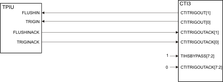 Figure 6-26 CTI3 Mapping
NOTE
TPIU and CTI3 run at different frequencies.
Table 6-49 CTI3 Mapping
| CTI TRIGGER | Module Signal |
|---|---|
| Trigger Input 0 | Reserved |
| Trigger Input 1 | Reserved |
| Trigger Input 2 | Reserved |
| Trigger Input 3 | Reserved |
| Trigger Input 4 | Reserved |
| Trigger Input 5 | Reserved |
| Trigger Input 6 | Reserved |
| Trigger Input 7 | Reserved |
| Trigger Output 0 | To TPIU TRIGIN |
| Trigger Output 1 | To TPIU FLUSHIN |
| Trigger Output 2 | Reserved |
| Trigger Output 3 | Reserved |
| Trigger Output 4 | Reserved |
| Trigger Output 5 | Reserved |
| Trigger Output 6 | Reserved |
| Trigger Output 7 | Reserved |
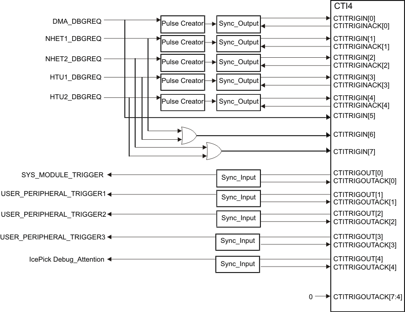 Figure 6-27 CTI4 Mapping
Table 6-50 CTI4 Mapping
| CTI TRIGGER | Module Signal |
|---|---|
| Trigger Input 0 | From DMA_DBGREQ |
| Trigger Input 1 | From N2HET1_DBGREQ |
| Trigger Input 2 | From N2HET2_DBGREQ |
| Trigger Input 3 | From HTU1_DBGREQ |
| Trigger Input 4 | From HTU2_DBGREQ |
| Trigger Input 5 | From DMA_DBGREQ |
| Trigger Input 6 | From N2HET1_DBGREQ or HTU1_DBGREQ |
| Trigger Input 7 | From N2HET2_DBGREQ or HTU2_DBGREQ |
| Trigger Output 0 | To SYS_MODULE_TRIGGER |
| Trigger Output 1 | To USER_PERIPHERAL_TRIGGER1 |
| Trigger Output 2 | To USER_PERIPHERAL_TRIGGER2 |
| Trigger Output 3 | To USER_PERIPHERAL_TRIGGER3 |
| Trigger Output 4 | To IcePick Debug_Attention |
| Trigger Output 5 | Reserved |
| Trigger Output 6 | Reserved |
| Trigger Output 7 | Reserved |
Table 6-51 Peripheral Suspend Generation
| TRIGGER OUTPUT | MODULE SIGNAL CONNECTED | DESCRIPTION |
|---|---|---|
| SYS_MODULE_TRIGGER | L2FMC_CPU_EMUSUSP | L2FMC Wrapper Suspend |
| CCM_R5_CPU_EMUSUSP | CCM_R5 module suspend | |
| CRC_CPU_EMUSUSP | CRC1 / CRC2 module suspend | |
| SYS_CPU_EMUSUSP | SYS module Suspend | |
| USER_PERIPHERAL_TRIGGER1 | DMA_SUSPEND | DMA Suspend |
| RTI_CPU_SUSPEND | RTI1 / RTI2 Suspend | |
| AWM_CPU_SUSPEND | AWM1 / AWM2 Suspend | |
| HTU_CPU_EMUSUSP | HTU1 / HTU2 Suspend | |
| SCI_CPU_EMUSUSP | SCI3 / SCI4 Suspend | |
| LIN_CPU_EMUSUSP | LIN1 / LIN2 Suspend | |
| I2C_CPU_EMUSUSP | I2C1 / I2C2 Suspend | |
| EMAC_CPU_EMUSUSP | EMAC Suspend | |
| EQEP_CPU_EMUSUSP | EQEP Suspend | |
| ECAP_CPU_EMUSUSP | ECAP Suspend | |
| DMM_CPU_EMUSUSP | DMM Suspend | |
| DCC_CPU_EMUSUSP | DCC1 / DCC2 Suspend | |
| USER_PERIPHERAL_TRIGGER2 | DCAN_CPU_EMUSUSP | DCAN1 / DCAN2 / DCAN3 / DCAN4 Suspend |
| USER_PERIPHERAL_TRIGGER3 | ePWM_CPU_EMUSUSP | ePWM1..7 Trip Zone TZ6n and ePWM1..7 Suspend |
6.22.4 JTAG Identification Code
The JTAG ID code for this device is the same as the device ICEPick Identification Code. For the JTAG ID Code per silicon revision, see Table 6-52.
Table 6-52 JTAG ID Code
| SILICON REVISION | ID |
|---|---|
| Rev A | 0x0B95A02F |
| Rev B | 0x1B95A02F |
6.22.5 Debug ROM
The Debug ROM stores the location of the components on the Debug APB bus (see Table 6-53).
Table 6-53 Debug ROM Table
| ADDRESS | DESCRIPTION | VALUE |
|---|---|---|
| 0x000 | Cortex-R5F | 0x00001003 |
| 0x004 | ETM-R5 | 0x00002003 |
| 0x008 | TPIU | 0x00003003 |
| 0x00C | POM | 0x00004003 |
| 0x018 | CTI1 | 0x00007003 |
| 0x020 | CTI3 | 0x00009003 |
| 0x024 | CTI4 | 0x0000A003 |
| 0x028 | CSTF | 0x0000B003 |
| 0x02C | end of table | 0x00000000 |
6.22.6 JTAG Scan Interface Timings
Table 6-54 JTAG Scan Interface Timing(1)
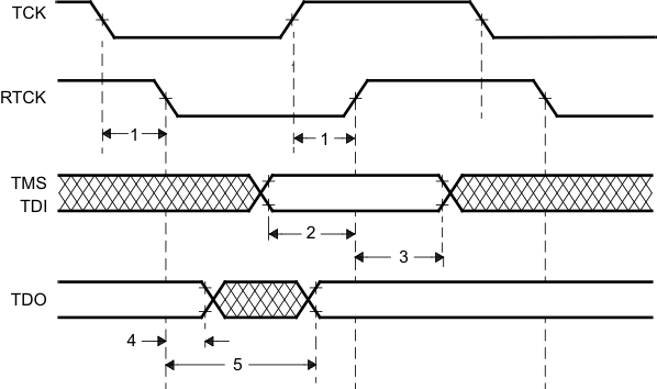 Figure 6-28 JTAG Timing
6.22.7 Advanced JTAG Security Module
This device includes a an Advanced JTAG Security Module (AJSM) module. The AJSM provides maximum security to the memory content of the device by letting users secure the device after programming.
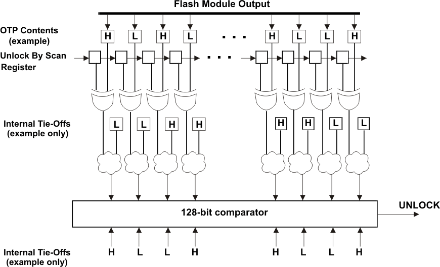 Figure 6-29 AJSM Unlock
The device is unsecure by default by virtue of a 128-bit visible unlock code programmed in the OTP address 0xF0000000. The OTP contents are XOR-ed with the contents of the "Unlock By Scan" register. The outputs of these XOR gates are again combined with a set of secret internal tie-offs. The output of this combinational logic is compared against a secret hard-wired 128-bit value. A match results in the UNLOCK signal being asserted, so that the device is now unsecure.
A user can secure the device by changing at least 1 bit in the visible unlock code from 1 to 0. Changing a 0 to 1 is not possible because the visible unlock code is stored in the One Time Programmable (OTP) flash region. Also, changing all 128 bits to zeros is not a valid condition and will permanently secure the device.
Once secured, a user can unsecure the device by scanning an appropriate value into the "Unlock By Scan" register of the AJSM. The value to be scanned is such that the XOR of the OTP contents and the Unlock-By-Scan register contents results in the original visible unlock code.
The Unlock-By-Scan register is reset only upon asserting power-on reset (nPORRST).
A secure device only permits JTAG accesses to the AJSM scan chain through the Secondary Tap 2 of the ICEPick module. All other secondary taps, test taps, and the boundary scan interface are not accessible in this state.
6.22.8 Embedded Trace Macrocell (ETM-R5)
The device contains a ETM-R5 module with a 32-bit internal data port. The ETM-R5 module is connected to a Trace Port Interface Unit (TPIU) with a 32-bit data bus. The TPIU provides a 35-bit (32-bit data, 3-bit control) external interface for trace. The ETM-R5 is CoreSight compliant and follows the ETM v3 specification. For more details, see the ARM CoreSight ETM-R5 TRM specification.
6.22.8.1 ETM TRACECLKIN Selection
The ETM clock source can be selected as either VCLK or the external ETMTRACECLKIN terminal. The selection is chosen by the EXTCTLOUT[1:0] control bits of the TPIU (default is '00'). The address of this register is the TPIU base address + 0x404.
Before the user begins accessing TPIU registers, the TPIU should be unlocked through the CoreSight key and 1 or 2 written to this register.
Table 6-55 TPIU / TRACECLKIN Selection
| EXTCTLOUT[1:0] | TPIU/TRACECLKIN |
|---|---|
| 00 | Tied-zero |
| 01 | VCLK |
| 10 | ETMTRACECLKIN |
| 11 | Tied-zero |
6.22.8.2 Timing Specifications
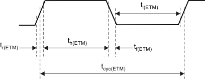 Figure 6-30 ETMTRACECLKOUT Timing
Table 6-56 ETMTRACECLK Timing
| PARAMETER | MIN | MAX | UNIT | |
|---|---|---|---|---|
| tcyc(ETM) | Clock period | 18.18 | ns | |
| tl(ETM) | Low pulse width | 6 | ns | |
| th(ETM) | High pulse width | 6 | ns | |
| tr(ETM) | Clock and data rise time | 3 | ns | |
| tf(ETM) | Clock and data fall time | 3 | ns | |
 Figure 6-31 ETMDATA Timing
Table 6-57 ETMDATA Timing
| PARAMETER | MIN | MAX | UNIT | |
|---|---|---|---|---|
| tsu(ETM) | Data setup time | 2.5 | ns | |
| th(ETM) | Data hold time | 1.5 | ns | |
NOTE
The ETMTRACECLK and ETMDATA timing is based on a 15-pF load and for ambient temperatures lower than 85°C.
6.22.9 RAM Trace Port (RTP)
The RTP provides the ability to datalog the RAM contents of the RM57Dx devices or accesses to peripherals without program intrusion. It can trace all data write or read accesses to internal RAM. In addition, it provides the capability to directly transfer data to a FIFO to support a CPU-controlled transmission of the data. The trace data is transmitted over a dedicated external interface.
6.22.9.1 RTP Features
The RTP offers the following features:
- Two modes of operation - Trace Mode and Direct Data Mode
- Trace Mode
- Nonintrusive data trace on write or read operation
- Visibility of RAM content at any time on external capture hardware
- Trace of peripheral accesses
- 2 configurable trace regions for each RAM module to limit amount of data to be traced
- FIFO to store data and address of data of multiple read/write operations
- Trace of CPU and/or DMA accesses with indication of the master in the transmitted data packet
- Direct Data Mode
- Directly write data with the CPU or trace read operations to a FIFO, without transmitting header and address information
- Trace Mode
- Dedicated synchronous interface to transmit data to external devices
- Free-running clock generation or clock stop mode between transmissions
- Up to 100 Mbps terminal transfer rate for transmitting data
- Pins not used in functional mode can be used as GIOs
6.22.9.2 Timing Specifications
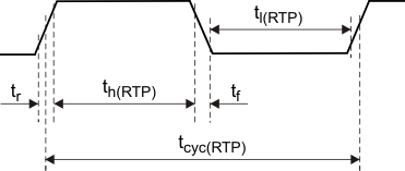 Figure 6-32 RTPCLK Timing
Table 6-58 RTPCLK Timing
| PARAMETER | MIN | MIN | UNIT | |
|---|---|---|---|---|
| tcyc(RTP) | Clock period | 9.09 (= 110 MHz) | ns | |
| th(RTP) | High pulse width | ((tcyc(RTP))/2) - ((tr+tf)/2) | ns | |
| tl(RTP) | Low pulse width | ((tcyc(RTP))/2) - ((tr+tf)/2) | ns | |
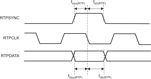 Figure 6-33 RTPDATA Timing
Table 6-59 RTPDATA Timing
| PARAMETER | MIN | MAX | UNIT | |
|---|---|---|---|---|
| tdsu(RTP) | Data setup time | 3 | ns | |
| tdh(RTP) | Data hold time | 1 | ns | |
| tssu(RTP) | SYNC setup time | 3 | ns | |
| tsh(RTP) | SYNC hold time | 1 | ns | |
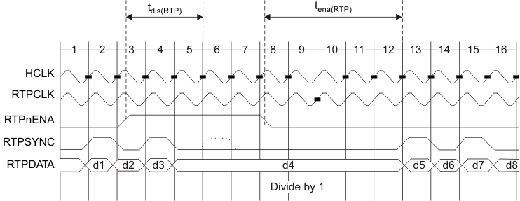 Figure 6-34 RTPnENA timing
Table 6-60 RTPnENA timing
| PARAMETER | MIN | MAX | UNIT | |
|---|---|---|---|---|
| tdis(RTP) | Disable time, time RTPnENA must go high before what would be the next RTPSYNC, to ensure delaying the next packet | 3tc(HCLK) + tr(RTPSYNC) + 12 | ns | |
| tena(RTP) | Enable time, time after RTPnENA goes low before a packet that has been halted, resumes | 4tc(HCLK) + tr(RTPSYNC) | 5tc(HCLK) + tr(RTPSYNC) + 12 | ns |
6.22.10 Data Modification Module (DMM)
The Data Modification Module (DMM) provides the capability to modify data in the entire 4GB address space of the RM57Dx devices from an external peripheral, with minimal interruption of the application.
6.22.10.1 DMM Features
The DMM module has the following features:
- Acts as a bus master, enabling direct writes to the 4GB address space without CPU intervention
- Writes to memory locations specified in the received packet (leverages packets defined by trace mode of the RAM Trace Port (RTP) module
- Writes received data to consecutive addresses, which are specified by the DMM module (leverages packets defined by direct data mode of the RTP module)
- Configurable port width (1-, 2-, 4-, 8-, 16-pins)
- Up to 100 Mbps terminal data rate
- Unused pins configurable as GIO pins
6.22.10.2 Timing Specifications
Table 6-61 DMMCLK Timing (see Figure 6-35)
| PARAMETER | MIN | MAX | UNIT | |
|---|---|---|---|---|
| tcyc(DMM) | Cycle time, DMMCLK clock period | 9.09 | ns | |
| th(DMM) | High-pulse width | ((tcyc(DMM))/2) - ((tr+tf)/2) | ns | |
| tl(DMM) | Low-pulse width | ((tcyc(DMM))/2) - ((tr+tf)/2) | ns | |
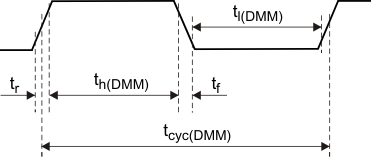 Figure 6-35 DMMCLK Timing
Table 6-62 DMMDATA Timing (see Figure 6-36)
| PARAMETER | MIN | MAX | UNIT | |
|---|---|---|---|---|
| tssu(DMM) | Setup time, SYNC active before clk falling edge | 2 | ns | |
| tsh(DMM) | Hold time, clk falling edge after SYNC deactive | 3 | ns | |
| tdsu(DMM) | Setup time, DATA before clk falling edge | 2 | ns | |
| tdh(DMM) | Hold time, clk falling edge after DATA hold time | 3 | ns | |
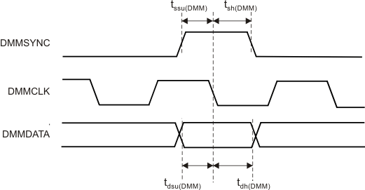 Figure 6-36 DMMDATA Timing
Figure 6-37 shows a case with 1 DMM packet per 2 DMMCLK cycles (Mode = Direct Data Mode, data width = 8, portwidth = 4) where none of the packets received by the DMM are sent out, leading to filling up of the internal buffers. The DMMnENA signal is shown asserted, after the first two packets have been received and synchronized to the HCLK domain. Here, the DMM has the capacity to accept packets D4x, D5x, D6x, D7x. Packet D8 would result in an overflow. Once DMMnENA is asserted, the DMM expects to stop receiving packets after 4 HCLK cycles; once DMMnENA is deasserted, the DMM can handle packets immediately (after 0 HCLK cycles).
 Figure 6-37 DMMnENA Timing
6.22.11 Boundary Scan Chain
The device supports BSDL-compliant boundary scan for testing pin-to-pin compatibility. The boundary scan chain is connected to the Boundary Scan Interface of the ICEPICK module (see Figure 6-38).
 Figure 6-38 Boundary Scan Implementation (Conceptual Diagram)
Data is serially shifted into all boundary-scan buffers through TDI, and out through TDO.
