ZHCSFB4A July 2016 – January 2024 DS90UB964-Q1
PRODUCTION DATA
- 1
- 1特性
- 2应用
- 3说明
- Pin Configuration and Functions
-
4Specifications
- 4.1 Absolute Maximum Ratings
- 4.2 ESD Ratings – JEDEC
- 4.3 ESD Ratings – IEC and ISO
- 4.4 Recommended Operating Conditions
- 4.5 Thermal Information
- 4.6 DC Electrical Characteristics
- 4.7 AC Electrical Characteristics
- 4.8 Recommended Timing for the Serial Control Bus
- 4.9 AC Electrical Characteristics
- 4.10 Typical Characteristics
-
5Detailed Description
- 5.1 Overview
- 5.2 Functional Block Diagram
- 5.3 Feature Description
- 5.4
Device Functional Modes
- 5.4.1 RAW Data Type Support and Rates
- 5.4.2 MODE Pin
- 5.4.3 REFCLK
- 5.4.4 Receiver Port Control
- 5.4.5 Input Jitter Tolerance
- 5.4.6 Adaptive Equalizer
- 5.4.7 Channel Monitor Loop-Through Output Driver
- 5.4.8 RX Port Status
- 5.4.9 GPIO Support
- 5.4.10 RAW Mode LV / FV Controls
- 5.4.11 Video Stream Forwarding
- 5.4.12 CSI-2 Protocol Layer
- 5.4.13 CSI-2 Short Packet
- 5.4.14 CSI-2 Long Packet
- 5.4.15 CSI-2 Data Identifier
- 5.4.16 Virtual Channel and Context
- 5.4.17 CSI-2 Mode Virtual Channel Mapping
- 5.4.18 CSI-2 Transmitter Frequency
- 5.4.19 CSI-2 Transmitter Status
- 5.4.20 Video Buffers
- 5.4.21 CSI-2 Line Count and Line Length
- 5.4.22 FrameSync Operation
- 5.4.23
CSI-2 Forwarding
- 5.4.23.1 Best-Effort Round Robin CSI-2 Forwarding
- 5.4.23.2 Synchronized CSI-2 Forwarding
- 5.4.23.3 Basic Synchronized CSI-2 Forwarding
- 5.4.23.4 Line-Interleaved CSI-2 Forwarding
- 5.4.23.5 Line-Concatenated CSI-2 Forwarding
- 5.4.23.6 CSI-2 Replicate Mode
- 5.4.23.7 CSI-2 Transmitter Output Control
- 5.4.23.8 Enabling and Disabling CSI-2 Transmitters
- 5.5
Programming
- 5.5.1 Serial Control Bus
- 5.5.2 Second I2C Port
- 5.5.3 I2C Target Operation
- 5.5.4 Remote Target Operation
- 5.5.5 Remote Target Addressing
- 5.5.6 Broadcast Write to Remote Devices
- 5.5.7 I2C Proxy Controller
- 5.5.8 I2C Proxy Controller Timing
- 5.5.9 Interrupt Support
- 5.5.10 Timestamp – Video Skew Detection
- 5.5.11 Pattern Generation
- 5.5.12 FPD-Link BIST Mode
- 5.6 Register Maps
- 6Application and Implementation
- 7Device and Documentation Support
- 8Revision History
- 9Mechanical, Packaging, and Orderable Information
5.4.17.2 Example 2
The DS90UB964-Q1 is receiving data from sensors attached to each port. Each port is sending a video stream. The DS90UB964-Q1 can be configured to map the VC-IDs and distribute to different CSI-2 Transmitters. This implementation maps VC-ID of 0 for RX Port 0, VC-ID of 1 for RX Port 1, VC-ID of 0 for RX Port 2, and VC-ID of 1 for RX Port 3. RX Ports 0 and 1 are assigned to CSI-2 Transmitter 0 which RX Ports 2 and 3 are assigned to CSI-2 Transmitter 1.
 Figure 5-11 VC-ID Mapping Example 2
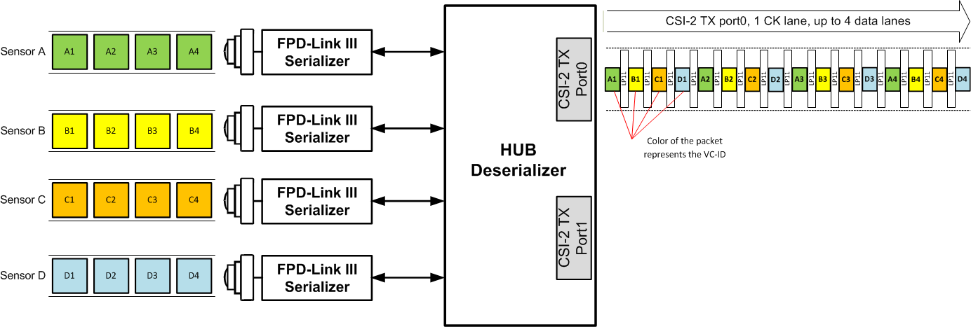
 Figure 5-12 Four
Sensor Data onto CSI-2 With Virtual Channels (VC-ID)
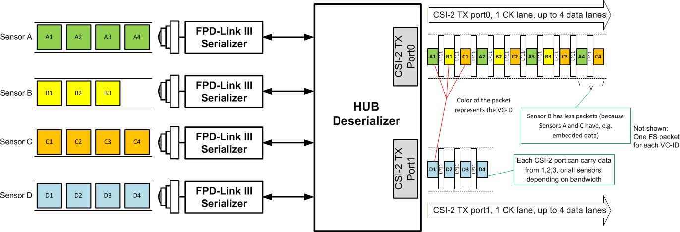
 Figure 5-13 Four
Sensor Data onto CSI-2 With Virtual Channels (VC-ID) With Different Frame
Size
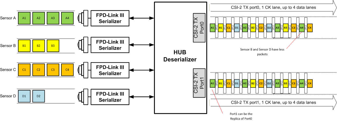
 Figure 5-14 Four
Sensor Data onto 1xCSI-2 Replicated With Virtual Channels (VC-ID) With Different
Frame Size