ZHCSFB5D July 2016 – December 2017 LM5141-Q1
PRODUCTION DATA.
- 1 特性
- 2 应用
- 3 说明
- 4 修订历史记录
- 5 Pin Configuration and Functions
- 6 Specifications
-
7 Detailed Description
- 7.1 Overview
- 7.2 Functional Block Diagram
- 7.3
Feature Description
- 7.3.1 High Voltage Start-up Regulator
- 7.3.2 VCC Regulator
- 7.3.3 Oscillator
- 7.3.4 Synchronization
- 7.3.5 Frequency Dithering (Spread Spectrum)
- 7.3.6 Enable
- 7.3.7 Power Good
- 7.3.8 Output Voltage
- 7.3.9 Current Sense
- 7.3.10 DCR Current Sensing
- 7.3.11 Error Amplifier and PWM Comparator
- 7.3.12 Slope Compensation
- 7.3.13 Hiccup Mode Current Limiting
- 7.3.14 Standby Mode
- 7.3.15 Soft Start
- 7.3.16 Diode Emulation
- 7.3.17 High- and Low-Side Drivers
-
8 Application and Implementation
- 8.1 Application Information
- 8.2 Typical Application
- 9 Power Supply Recommendations
- 10Layout
- 11器件和文档支持
- 12机械、封装和可订购信息
7.3.5 Frequency Dithering (Spread Spectrum)
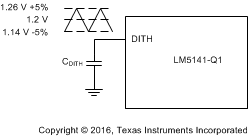
The LM5141-Q1 provides a frequency dithering option that is enabled by connecting a capacitor from the DITH pin to AGND. A triangular waveform centered at 1.2 V is generated across the CDITH capacitor. Refer to Figure 22. The triangular waveform modulates the oscillator frequency by ±5% of the nominal frequency set by the OSC pin or by an RT resistor. The CDITH capacitance value sets the rate of the low frequency modulation. A lower CDITH capacitance will modulate the oscillator frequency at a faster rate than a higher capacitance. For the dithering circuit to effectively reduce the peak EMI, the modulation rate must be less than the oscillator frequency (FSW). Equation 3 calculates the DITH pin capacitance required to set the modulation frequency, FMOD.

If the DITH pin is connected to VDDA during power-up the dither feature is latch-off and cannot be changed unless VCC is allowed to drop below the VCC(UVLO) threshold. If the DITH pin is connected to ground on power up, dither will be disabled, but it can be enabled by raising the DITH pin voltage above ground and connecting it to CDITH. When the LM5141 is synchronized to an external clock, Dither is disabled.
 Figure 22. Dither Operation