ZHCSFF5G July   2016  – December  2019 TPS2660

PRODUCTION DATA.  

  1. 特性
  2. 应用
    1.     简化电路原理图
  3. 说明
    1.     –60V 电源时的反向输入极性保护
  4. 修订历史记录
  5. Device Comparison Table
  6. Pin Configuration and Functions
    1.     Pin Functions
  7. Specifications
    1. 7.1 Absolute Maximum Ratings
    2. 7.2 ESD Ratings
    3. 7.3 Recommended Operating Conditions
    4. 7.4 Thermal Information
    5. 7.5 Electrical Characteristics
    6. 7.6 Timing Requirements
    7. 7.7 Typical Characteristics
  8. Parameter Measurement Information
  9. Detailed Description
    1. 9.1 Overview
    2. 9.2 Functional Block Diagram
    3. 9.3 Feature Description
      1. 9.3.1 Undervoltage Lockout (UVLO)
      2. 9.3.2 Overvoltage Protection (OVP)
      3. 9.3.3 Reverse Input Supply Protection
      4. 9.3.4 Hot Plug-In and In-Rush Current Control
      5. 9.3.5 Overload and Short Circuit Protection
        1. 9.3.5.1 Overload Protection
          1. 9.3.5.1.1 Active Current Limiting
          2. 9.3.5.1.2 Electronic Circuit Breaker with Overload Timeout, MODE = OPEN
        2. 9.3.5.2 Short Circuit Protection
          1. 9.3.5.2.1 Start-Up With Short-Circuit On Output
        3. 9.3.5.3 FAULT Response
          1. 9.3.5.3.1 Look Ahead Overload Current Fault Indicator
        4. 9.3.5.4 Current Monitoring
        5. 9.3.5.5 IN, OUT, RTN, and GND Pins
        6. 9.3.5.6 Thermal Shutdown
        7. 9.3.5.7 Low Current Shutdown Control (SHDN)
    4. 9.4 Device Functional Modes
  10. 10Application and Implementation
    1. 10.1 Application Information
    2. 10.2 Typical Application
      1. 10.2.1 Design Requirements
      2. 10.2.2 Detailed Design Procedure
        1. 10.2.2.1 Step by Step Design Procedure
        2. 10.2.2.2 Programming the Current-Limit Threshold—R(ILIM) Selection
        3. 10.2.2.3 Undervoltage Lockout and Overvoltage Set Point
        4. 10.2.2.4 Programming Current Monitoring Resistor—RIMON
        5. 10.2.2.5 Setting Output Voltage Ramp Time—(tdVdT)
          1. 10.2.2.5.1 Case 1: Start-Up Without Load—Only Output Capacitance C(OUT) Draws Current During Start-Up
          2. 10.2.2.5.2 Case 2: Start-Up With Load—Output Capacitance C(OUT) and Load Draws Current During Start-Up
          3. 10.2.2.5.3 Support Component Selections—RFLTb and C(IN)
      3. 10.2.3 Application Curves
    3. 10.3 System Examples
      1. 10.3.1 Acive ORing Operation
      2. 10.3.2 Field Supply Protection in PLC, DCS I/O Modules
      3. 10.3.3 Simple 24-V Power Supply Path Protection
    4. 10.4 Do's and Don'ts
  11. 11Power Supply Recommendations
    1. 11.1 Transient Protection
  12. 12Layout
    1. 12.1 Layout Guidelines
    2. 12.2 Layout Example
  13. 13器件和文档支持
    1. 13.1 器件支持
    2. 13.2 文档支持
      1. 13.2.1 相关文档
    3. 13.3 接收文档更新通知
    4. 13.4 社区资源
    5. 13.5 商标
    6. 13.6 静电放电警告
    7. 13.7 Glossary
  14. 14机械、封装和可订购信息

Active Current Limiting

When the active current limiting mode is selected, during overload events, the device continuously regulates the load current to the overcurrent limit I(OL) programmed by the R(ILIM) resistor as shown in Equation 3.

Equation 3. TPS2660 equ_04_SLVSDG2.gif

where

  • I(OL) is the overload current limit in Ampere
  • R(ILIM) is the current limit resistor in kΩ

During an overload condition, the internal current-limit amplifier regulates the output current to I(LIM). The FLT signal assert after a delay of 875 µs.The output voltage droops during the current regulation, resulting in increased power dissipation in the device. If the device junction temperature reaches the thermal shutdown threshold (T(TSD)), the internal FET is turn off. The device configured in latch-off mode stays latched off until it is reset by either of the following conditions:

  • Cycling V(IN) below V(PORF)
  • Toggling SHDN

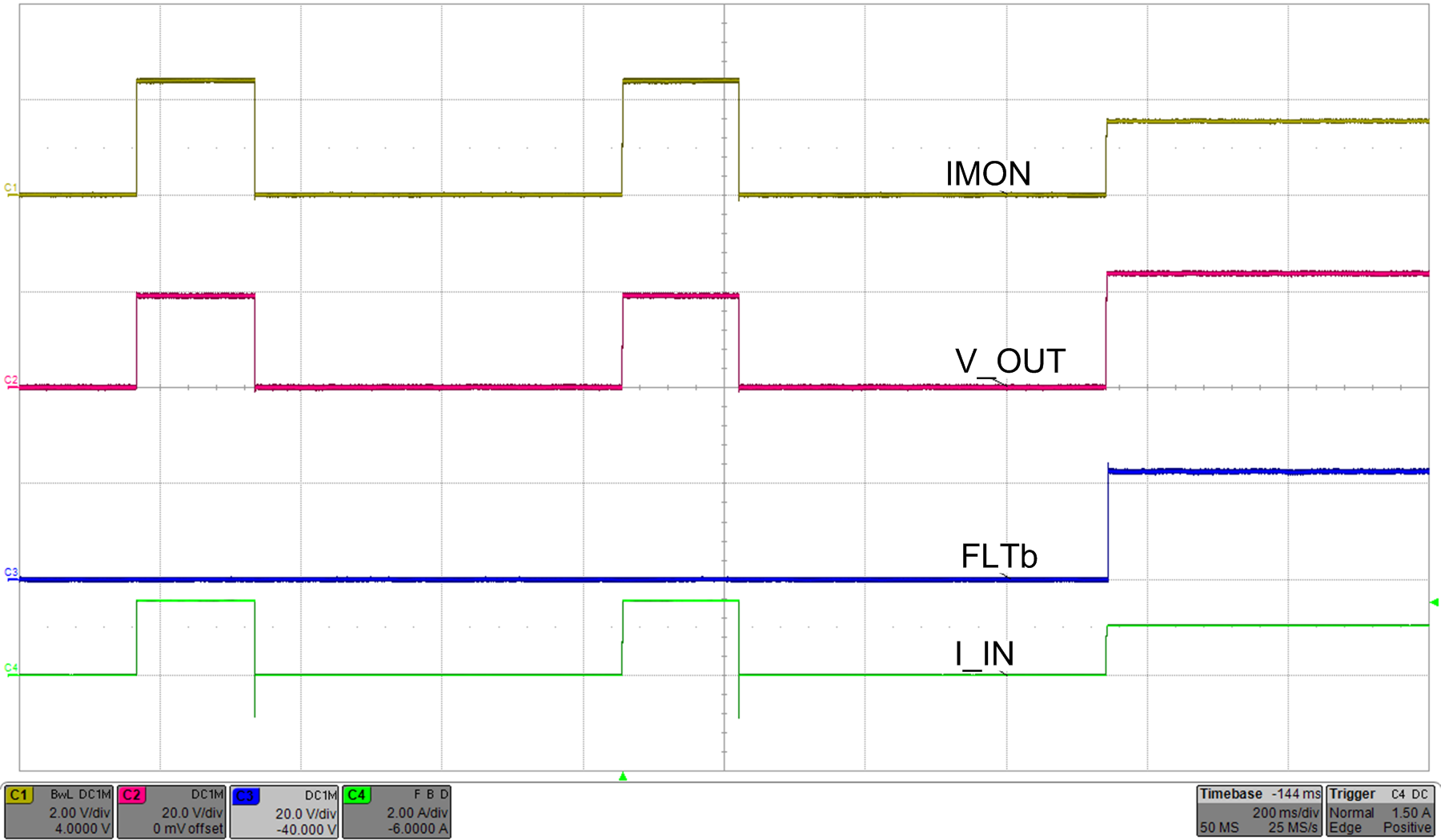
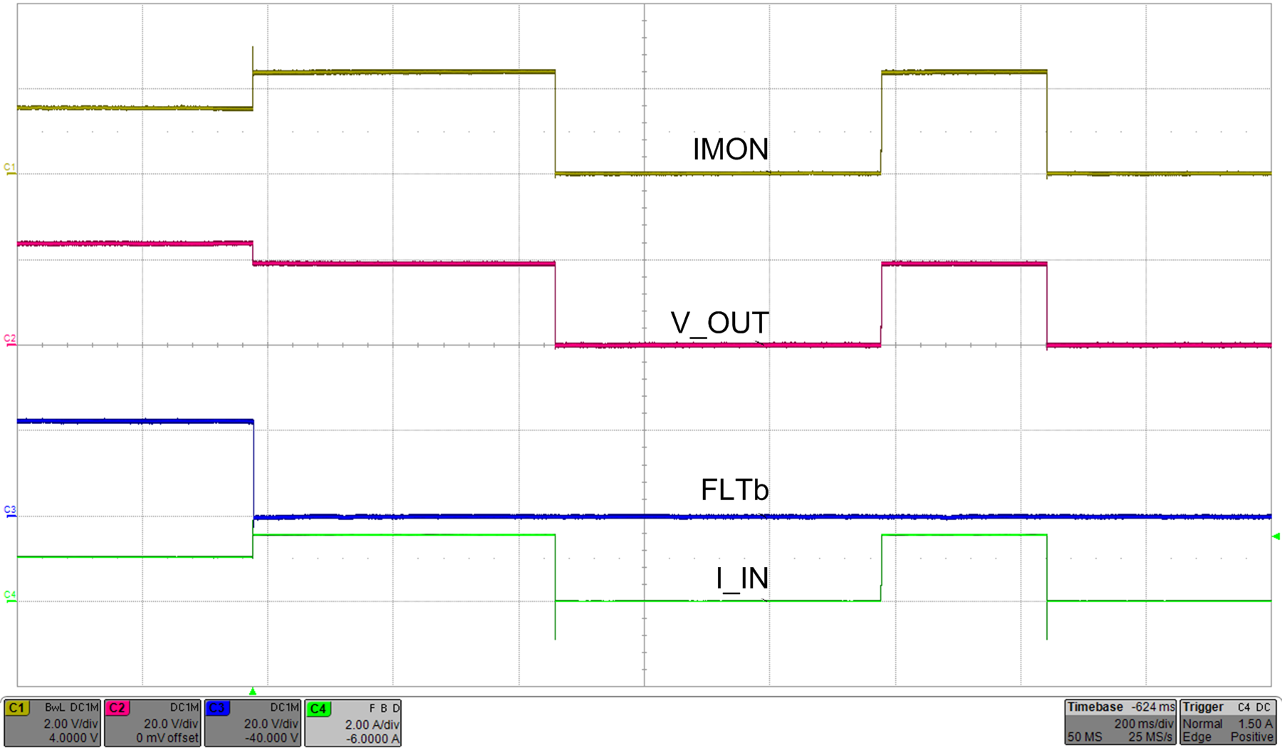
Whereas the device configured in auto-retry mode, commences an auto-retry cycle 512 ms after TJ < [T(TSD) – 10°C]. The FLT signal remains asserted until the fault condition is removed and the device resumes normal operation. Figure 39 and Figure 40 illustrates behavior of the system during current limiting with auto-retry functionality.
TPS2660 scope_shot_01_slvsdg2.png
Load transition from 22 Ω to 12 Ω MODE pin connected to RTN
RILIM = 8 kΩ
Figure 39. Auto-Retry MODE Fault Behavior
TPS2660 scope_shot_02_slvsdg2.png
RILIM = 5.36 kΩ
Figure 40. Response During Coming Out of Overload Fault