ZHCSFF5G July 2016 – December 2019 TPS2660
PRODUCTION DATA.
- 1 特性
- 2 应用
- 3 说明
- 4 修订历史记录
- 5 Device Comparison Table
- 6 Pin Configuration and Functions
- 7 Specifications
- 8 Parameter Measurement Information
-
9 Detailed Description
- 9.1 Overview
- 9.2 Functional Block Diagram
- 9.3
Feature Description
- 9.3.1 Undervoltage Lockout (UVLO)
- 9.3.2 Overvoltage Protection (OVP)
- 9.3.3 Reverse Input Supply Protection
- 9.3.4 Hot Plug-In and In-Rush Current Control
- 9.3.5 Overload and Short Circuit Protection
- 9.4 Device Functional Modes
-
10Application and Implementation
- 10.1 Application Information
- 10.2
Typical Application
- 10.2.1 Design Requirements
- 10.2.2 Detailed Design Procedure
- 10.2.3 Application Curves
- 10.3 System Examples
- 10.4 Do's and Don'ts
- 11Power Supply Recommendations
- 12Layout
- 13器件和文档支持
- 14机械、封装和可订购信息
10.2.2.5.2 Case 2: Start-Up With Load—Output Capacitance C(OUT) and Load Draws Current During Start-Up
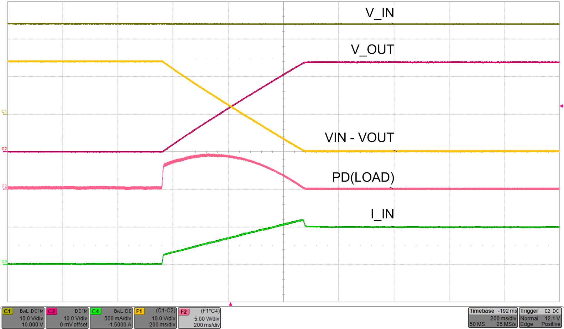
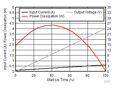
When the load draws current during the turnon sequence, additional power is dissipated in the device. Considering a resistive load RL(SU) during start-up, typical ramp-up of output voltage, load current and the instantaneous power dissipation in the device are shown in Figure 53. Instantaneous power dissipation with respect to time is plotted in Figure 54. The additional power dissipation during start-up is calculated using Equation 17.

| VIN = 24 V | RL(SU) = 48 Ω | ||
| CdVdT = 2.2 µF | COUT = 2.2 mF | ||

| VIN = 24 V | RL(SU) = 48 Ω | ||
| CdVdT = 2.2 µF | COUT = 2.2 mF | ||

Total power dissipated in the device during start-up is given by Equation 18.

Total current during start-up is given by Equation 19.

For the design example under discussion,
Select the inrush current I(INRUSH) = 0.1 A and calculate tdVdT using Equation 20.

For a given start-up time, CdVdT capacitance value is calculated using Equation 21.

where
- t(dVdT) = 0.528 s
- V(IN) = 24 V
Choose the closest standard value: 2.2-µF/16-V capacitor.
The inrush power dissipation is calculated, using Equation 22.

where
- V(IN) = 24 V
- I(INRUSH) = 0.1 A
Considering the start-up with 48-Ω load, the additional power dissipation, is calculated using Equation 23.

where
- V(IN) = 24 V
- RL(SU) = 48 Ω
The total device power dissipation during start-up is given by Equation 24.

where
- PD(INRUSH) = 1.2 W
- PD(LOAD) = 2 W
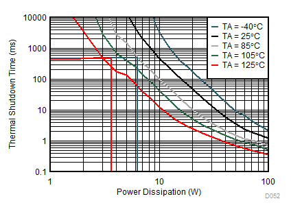
The power dissipation with or without load, for a selected start-up time must not exceed the thermal shutdown limits as shown in Figure 55.
From the thermal shutdown limit graph, at TA = 85°C, thermal shutdown time for 3.2 W is close to 28000 ms. It is safe to have a minimum 30% margin to allow for variation of the system parameters such as load, component tolerance, input voltage and layout. Selected 2.2-µF CdVdT capacitor and 528-ms start-up time (tdVdT) are within limit for successful start-up with 48-Ω load.
Higher value C(dVdT) capacitor can be selected to further reduce the power dissipation during start-up.
 Figure 55. Thermal Shutdown Time vs Power Dissipation