ZHCSFH5A March 2016 – September 2016 ISO7821LLS
PRODUCTION DATA.
- 1 特性
- 2 应用
- 3 说明
- 4 修订历史记录
- 5 Pin Configuration and Functions
-
6 Specifications
- 6.1 Absolute Maximum Ratings
- 6.2 ESD Ratings
- 6.3 Recommended Operating Conditions
- 6.4 Thermal Information
- 6.5 Power Ratings
- 6.6 Insulation Specifications
- 6.7 Safety-Related Certifications
- 6.8 Safety Limiting Values
- 6.9 DC Electrical Characteristics
- 6.10 DC Supply Current Characteristics
- 6.11 Timing Requirements for Distortion Correction Scheme
- 6.12 Switching Characteristics
- 6.13 Insulation Characteristics Curves
- 6.14 Typical Characteristics
- 7 Parameter Measurement Information
- 8 Detailed Description
- 9 Application and Implementation
- 10Power Supply Recommendations
- 11Layout
- 12器件和文档支持
- 13机械、封装和可订购信息
6 Specifications
6.1 Absolute Maximum Ratings
over operating free-air temperature range (unless otherwise noted)(1)| MIN | MAX | UNIT | |||
|---|---|---|---|---|---|
| VCCx | Supply voltage(2) | VCC1, VCC2 | –0.5 | 6 | V |
| V | Voltage on input, output, and enable pins | OUTx, INx, ENx | –0.5 | VCCx + 0.5(3) | V |
| IO | Maximum current through OUTx pins | –20 | 20 | mA | |
| TJ | Junction temperature | –55 | 150 | °C | |
| Tstg | Storage temperature | –65 | 150 | °C | |
(1) Stresses beyond those listed under Absolute Maximum Ratings may cause permanent damage to the device. These are stress ratings only, which do not imply functional operation of the device at these or any other conditions beyond those indicated under Recommended Operating Conditions. Exposure to absolute-maximum-rated conditions for extended periods may affect device reliability.
(2) All voltage values except differential I/O bus voltages are with respect to the local ground pin (GND1 or GND2) and are peak voltage values.
(3) Maximum voltage must not exceed 6 V.
6.2 ESD Ratings
| VALUE | UNIT | |||
|---|---|---|---|---|
| V(ESD) | Electrostatic discharge | Human-body model (HBM), per ANSI/ESDA/JEDEC JS-001(1) | ±4500 | V |
| Charged-device model (CDM), per JEDEC specification JESD22-C101(2) | ±1500 | |||
(1) JEDEC document JEP155 states that 500-V HBM allows safe manufacturing with a standard ESD control process.
(2) JEDEC document JEP157 states that 250-V CDM allows safe manufacturing with a standard ESD control process.
6.3 Recommended Operating Conditions
| MIN | NOM | MAX | UNIT | |||
|---|---|---|---|---|---|---|
| VCC1, VCC2 | Supply voltage | 3 | 3.3 | 5.5 | V | |
| |VID| | Magnitude of RX input differential voltage | Driven with voltage sources on RX pins | 100 | 600 | mV | |
| VIC | RX input common-mode voltage | VCC1, VCC2 ≥ 3 V | 0.5 |VID| | 2.4 – 0.5 |VID| | V | |
| RL | TX far-end differential termination | 100 | Ω | |||
| DR | Signaling rate | 50 | 150 | Mbps | ||
| TA | Ambient temperature | –55 | 25 | 125 | °C | |
6.4 Thermal Information
| THERMAL METRIC(1) | ISO7821LLS | UNIT | |||
|---|---|---|---|---|---|
| DW (SOIC) | DWW (SOIC) | ||||
| 16 PINS | 16 PINS | ||||
| RθJA | Junction-to-ambient thermal resistance | 82 | 84.6 | °C/W | |
| RθJC(top) | Junction-to-case(top) thermal resistance | 44.6 | 46.4 | °C/W | |
| RθJB | Junction-to-board thermal resistance | 46.6 | 55.3 | °C/W | |
| ψJT | Junction-to-top characterization parameter | 17.8 | 18.7 | °C/W | |
| ψJB | Junction-to-board characterization parameter | 46.1 | 54.5 | °C/W | |
| RθJC(bottom) | Junction-to-case(bottom) thermal resistance | — | — | °C/W | |
(1) For more information about traditional and new thermal metrics, see the Semiconductor and IC Package Thermal Metrics application report.
6.5 Power Ratings
VCC1 = VCC2 = 5.5 V, TJ = 150°C, CL = 5 pF, RL = 100-Ω differential, input a 75-MHz 50% duty-cycle square wave,EN1 = EN2 = 5.5 V
| PARAMETER | TEST CONDITIONS | MAX | TYP | MAX | UNIT | |
|---|---|---|---|---|---|---|
| PD | Maximum power dissipation (both sides) | 180 | mW | |||
| PD1 | Maximum power dissipation (side 1) | 90 | mW | |||
| PD2 | Maximum power dissipation (side 2) | 90 | mW | |||
6.6 Insulation Specifications
over operating free-air temperature range (unless otherwise noted)| PARAMETER | TEST CONDITIONS | SPECIFICATION | UNIT | ||
|---|---|---|---|---|---|
| DW | DWW | ||||
| GENERAL | |||||
| CLR | External clearance(1) | Shortest terminal-to-terminal distance through air | >8 | >14.5 | mm |
| CPG | External creepage(1) | Shortest terminal-to-terminal distance across the package surface | >8 | >14.5 | mm |
| DTI | Distance through the insulation | Minimum internal gap (internal clearance) | >21 | >21 | μm |
| CTI | Tracking resistance (comparative tracking index) | DIN EN 60112 (VDE 0303–11); IEC 60112; UL 746A | >600 | >600 | V |
| Material group | According to IEC 60664-1 | I | I | ||
| Overvoltage category per IEC 60664-1 | Rated mains voltage ≤ 600 VRMS | I–IV | I–IV | ||
| Rated mains voltage ≤ 1000 VRMS | I–III | I–IV | |||
| DIN V VDE V 0884–10 (VDE V 0884–10):2006–12(2) | |||||
| VIORM | Maximum repetitive peak isolation voltage | AC voltage (bipolar) | 2121 | 2828 | VPK |
| VIOWM | Maximum isolation working voltage | AC voltage (sine wave); time dependent dielectric breakdown (TDDB) test; see Figure 1 and Figure 2 | 1500 | 2000 | VRMS |
| DC voltage | 2121 | 2828 | VDC | ||
| VIOTM | Maximum transient isolation voltage | VTEST = VIOTM, t = 60 s (qualification) t = 1 s (100% production) |
8000 | 8000 | VPK |
| VIOSM | Maximum surge isolation voltage(3) | Test method per IEC 60065, 1.2/50 µs waveform, VTEST = 1.6 × VIOSM = 12800 VPK (qualification) |
8000 | 8000 | VPK |
| qpd | Apparent charge(4) | Method a: After I/O safety test subgroup 2/3, Vini = VIOTM, tini = 60 s; Vpd(m) = 1.2 × VIORM = 2545 VPK (DW) and 3394 VPK (DWW), tm = 10 s |
≤5 | ≤5 | pC |
| Method a: After environmental tests subgroup 1, Vini = VIOTM, tini = 60 s; Vpd(m) = 1.6 × VIORM = 3394 VPK (DW) and 4525 VPK (DWW), tm = 10 s |
≤5 | ≤5 | |||
| Method b1: At routine test (100% production) and preconditioning (type test) Vini = VIORM, tini = 1 s; Vpd(m) = 1.875 × VIORM= 3977 VPK (DW) and 5303 VPK (DWW), tm = 1 s |
≤5 | ≤5 | |||
| CIO | Barrier capacitance, input to output(5) | VIO = 0.4 × sin (2πft), f = 1 MHz | ~0.7 | ~0.7 | pF |
| RIO | Isolation resistance, input to output(5) | VIO = 500 V, TA = 25°C | >1012 | >1012 | Ω |
| VIO = 500 V, 100°C ≤ TA ≤ 125°C | >1011 | >1011 | |||
| VIO = 500 V at TS = 150°C | >109 | >109 | |||
| Pollution degree | 2 | 2 | |||
| Climatic category | 55/125/21 | 55/125/21 | |||
| UL 1577 | |||||
| VISO | Withstanding isolation voltage | VTEST = VISO = 5700 VRMS, t = 60 s (qualification); VTEST = 1.2 × VISO = 6840 VRMS, t = 1 s (100% production) |
5700 | 5700 | VRMS |
(1) Creepage and clearance requirements should be applied according to the specific equipment isolation standards of an application. Care should be taken to maintain the creepage and clearance distance of a board design to ensure that the mounting pads of the isolator on the printed-circuit board do not reduce this distance. Creepage and clearance on a printed-circuit board become equal in certain cases. Techniques such as inserting grooves and/or ribs on a printed circuit board are used to help increase these specifications.
(2) This coupler is suitable for safe electrical insulation only within the safety ratings. Compliance with the safety ratings shall be ensured by means of suitable protective circuits.
(3) Testing is carried out in air or oil to determine the intrinsic surge immunity of the isolation barrier.
(4) Apparent charge is electrical discharge caused by a partial discharge (pd).
(5) All pins on each side of the barrier tied together creating a two-terminal device.
6.7 Safety-Related Certifications
| VDE | CSA | UL | CQC | TUV |
|---|---|---|---|---|
| Plan to certify according to DIN V VDE V 0884-10 (VDE V 0884-10):2006-12 and DIN EN 60950-1 (VDE 0805 Teil 1):2011-01 | Plan to certify under CSA Component Acceptance Notice 5A, IEC 60950-1 and IEC 60601-1 | Plan to certify according to UL 1577 Component Recognition Program | Plan to certify according to GB 4943.1-2011 | Plan to certify according to EN 61010-1:2010 (3rd Ed) and EN 60950-1:2006/A11:2009/A1:2010/ A12:2011/A2:2013 |
| Reinforced insulation Maximum transient isolation voltage, 8000 VPK; Maximum repetitive peak isolation voltage, 2121 VPK (DW), 2828 VPK (DWW); Maximum surge isolation voltage, 8000 VPK |
Reinforced insulation per CSA 60950-1-07+A1+A2 and IEC 60950-1 2nd Ed., 800 VRMS (DW package) and 1450 VRMS (DWW package) max working voltage (pollution degree 2, material group I); | Single protection, 5700 VRMS |
Reinforced Insulation, Altitude ≤ 5000 m, Tropical Climate, 250 VRMS maximum working voltage | 5700 VRMS Reinforced insulation per EN 61010-1:2010 (3rd Ed) up to working voltage of 600 VRMS (DW package) and 1000 VRMS (DWW package) |
| 2 MOPP (Means of Patient Protection) per CSA 60601-1:14 and IEC 60601-1 Ed. 3.1, 250 VRMS (354 VPK) max working voltage (DW package) | 5700 VRMS Reinforced insulation per EN 60950-1:2006/A11:2009/A1:2010/ A12:2011/A2:2013 up to working voltage of 800 VRMS (DW package) and 1450 VRMS (DWW package) |
|||
| Certification planned | Certification planned | Certification planned | Certification planned | Certification planned |
6.8 Safety Limiting Values
Safety limiting intends to minimize potential damage to the isolation barrier upon failure of input or output circuitry. A failure of the I/O can allow low resistance to ground or the supply and, without current limiting, dissipate sufficient power to overheat the die and damage the isolation barrier potentially leading to secondary system failures.| PARAMETER | TEST CONDITIONS | MIN | TYP | MAX | UNIT | |
|---|---|---|---|---|---|---|
| DW PACKAGE | ||||||
| IS | Safety input, output, or supply current | RθJA = 82°C/W, VI = 5.5 V, TJ = 150°C, TA = 25°C, see Figure 3 |
277 | mA | ||
| RθJA = 82°C/W, VI = 3.6 V, TJ = 150°C, TA = 25°C, see Figure 3 |
423 | |||||
| PS | Safety input, output, or total power | RθJA = 82°C/W, TJ = 150°C, TA = 25°C, see Figure 5 |
1524 | mW | ||
| TS | Maximum safety temperature | 150 | °C | |||
| DWW PACKAGE | ||||||
| IS | Safety input, output, or supply current | RθJA = 84.6°C/W, VI = 5.5 V, TJ = 150°C, TA = 25°C, see Figure 4 |
269 | mA | ||
| RθJA = 84.6°C/W, VI = 3.6 V, TJ = 150°C, TA = 25°C, see Figure 4 |
410 | |||||
| PS | Safety input, output, or total power | RθJA = 84.6°C/W, TJ = 150°C, TA = 25°C, see Figure 6 |
1478 | mW | ||
| TS | Maximum safety temperature | 150 | °C | |||
The maximum safety temperature is the maximum junction temperature specified for the device. The power dissipation and junction-to-air thermal impedance of the device installed in the application hardware determines the junction temperature. The assumed junction-to-air thermal resistance in the Thermal Information is that of a device installed on a High-K test board for leaded surface-mount packages. The power is the recommended maximum input voltage times the current. The junction temperature is then the ambient temperature plus the power times the junction-to-air thermal resistance.
6.9 DC Electrical Characteristics
(over recommended operating conditions unless otherwise noted)| PARAMETER | TEST CONDITIONS | MIN | TYP | MAX | UNIT | |
|---|---|---|---|---|---|---|
| GENERAL | ||||||
| IIN(EN) | Leakage Current on ENx pins | Internal pullup on ENx pins | 13 | 40 | µA | |
| VCC+(UVLO) | Positive-going undervoltage-lockout (UVLO) threshold | 2.25 | V | |||
| VCC–(UVLO) | Negative-going UVLO threshold | 1.7 | V | |||
| VHYS(UVLO) | UVLO threshold hysteresis | 0.2 | V | |||
| VEN(ON) | EN pin turn-on threshold | 0.7 VCCx | V | |||
| VEN(OFF) | EN pin turn-off threshold | 0.3 VCCx | V | |||
| VEN(HYS) | EN pin threshold hysteresis | 0.1 VCCx | V | |||
| CMTI | Common-mode transient immunity | VI = VCCI(1) or 0 V; VCM = 1000 V, see Figure 22 |
100 | 120 | kV/μs | |
| LVDS TX | ||||||
| |VOD| | TX DC output differential voltage | RL = 100 Ω, see Figure 23 | 250 | 350 | 450 | mV |
| ∆VOD | Change in TX DC output differential between logic 1 and 0 states | RL = 100 Ω, see Figure 23 | –10 | 0 | 10 | mV |
| VOC | TX DC output common-mode voltage | RL = 100 Ω, see Figure 23 | 1.125 | 1.2 | 1.375 | V |
| ∆VOC | TX DC common-mode voltage difference | RL = 100 Ω, see Figure 23 | –25 | 0 | 25 | mV |
| IOS | TX output short circuit current through OUTx | OUTx = 0 | 10 | mA | ||
| OUTxP = OUTxM | 10 | |||||
| IOZ | TX output current when in high impedance | ENx = 0, OUTx from 0 to VCCx | –5 | 5 | µA | |
| COUT | TX output pad capacitance on OUTx at 1 MHz | DW package: ENx = 0, DC offset = VCC / 2, Swing = 200 mV, Frequency (f) = 1 MHz |
10 | pF | ||
| DWW package: ENx = 0, DC offset = VCC / 2, Swing = 200 mV, Frequency (f) = 1 MHz |
10 | |||||
| LVDS RX | ||||||
| VIC | RX input common mode voltage | VCCx ≥ 3 V | 0.5 |VID| | 1.2 | 2.4 – 0.5 |VID| | V |
| VIT1 | Positive going RX input differential threshold | Across VIC | 50 | mV | ||
| VIT2 | Negative going RX input differential threshold | Across VIC | –50 | mV | ||
| IINx | Input current on INx | From 0 to VCC (each input independently) | 10 | 20 | µA | |
| IINxP – IINxM | Input current balance | From 0 to VCC | –6 | 6 | µA | |
| CIN | RX input pad capacitance on INx at 1 MHz | DW package: DC offset = 1.2 V, Swing = 200 mV, f = 1 MHz |
6.6 | pF | ||
| DWW package: DC offset = 1.2 V, Swing = 200 mV, f = 1 MHz |
7.5 | |||||
(1) VCCI = Input-side VCCx; VCCO = Output-side VCCx.
6.10 DC Supply Current Characteristics
(over recommended operating conditions unless otherwise noted)| PARAMETER | TEST CONDITIONS | MIN | TYP | MAX | UNIT | ||
|---|---|---|---|---|---|---|---|
| ICC1
ICC2 |
Supply current side 1 and side 2 |
3 V < VCC1, VCC2 < 3.6 V | EN1 = EN2 = 0, OUTx floating, VID ≥ 50 mV | 2.3 | 3.6 | mA | |
| EN1 = EN2 = 0, OUTx floating, VID ≤ –50 mV | 3.5 | 5.6 | |||||
| EN1 = EN2 = 1, RL = 100-Ω differential, VID ≥ 50 mV | 6.2 | 9.9 | |||||
| EN1 = EN2 = 1, RL = 100-Ω differential, VID ≤ –50 mV | 7.5 | 12 | |||||
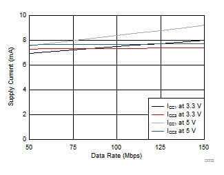
| EN1 = EN2 = 1, RL = 100-Ω differential, data communication at 50 Mbps |
7.6 | 12.1 | |||||
| EN1 = EN2 = 1, RL = 100-Ω differential, data communication at 125 Mbps |
8.5 | 13.6 | |||||
| EN1 = EN2 = 1, RL = 100-Ω differential, data communication at 150 Mbps |
8.9 | 14.2 | |||||
| 4.5 V < VCC1, VCC2 < 5.5 V | EN1 = EN2 = 0, OUTx floating, VID ≥ 50 mV | 2.3 | 3.6 | ||||
| EN1 = EN2 = 0, OUTx floating, VID ≤ –50 mV | 3.6 | 5.7 | |||||
| EN1 = EN2 = 1, RL = 100-Ω differential, VID ≥ 50 mV | 6.6 | 10.5 | |||||
| EN1 = EN2 = 1, RL = 100-Ω differential, VID ≤ –50 mV | 7.9 | 12.6 | |||||
| EN1 = EN2 = 1, RL = 100-Ω differential, data communication at 50 Mbps |
8.3 | 13.2 | |||||
| EN1 = EN2 = 1, RL = 100-Ω differential, data communication at 125 Mbps |
9.7 | 15.5 | |||||
| EN1 = EN2 = 1, RL = 100-Ω differential, data communication at 150 Mbps |
10.3 | 16.4 | |||||
6.11 Timing Requirements for Distortion Correction Scheme
Valid data = 8b10b like data with DC balance and bounded disparity. See Figure 25.| MIN | NOM | MAX | UNIT | ||
|---|---|---|---|---|---|
| tCALIB | Time to complete internal calibration, after exiting idle state. LVDS TX output is held high during this time. During this time valid data must be presented at the receiver. | 250 | 750 | µs | |
| tIDLE | The minimum duration of any idle state that must be maintained between valid data transmissions. | 10 | µs | ||
| tIDLE_OUT | After a channel enters idle state, the internal calibration loses lock after this time, and the LVDS outputs are gated high. | 200 | 600 | ns | |
6.12 Switching Characteristics
(over recommended operating conditions unless otherwise noted)| PARAMETER | TEST CONDITIONS | MIN | TYP | MAX | UNIT | |
|---|---|---|---|---|---|---|
| LVDS CHANNEL | ||||||
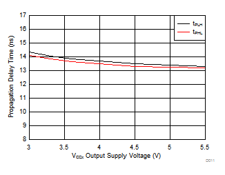
| tPLH
tPHL |
Propagation delay time | 17 | 25 | ns | ||
| tsk(o) | Channel-to-channel output skew time | Opposite directional channels, same voltage and temperature | 4.5 | ns | ||
| tsk(pp) | Part-part skew | Same directional channels, same voltage and temperature | 4.5 | ns | ||
| tCMset | Common-mode setting time after EN = 0 to EN = 1 transition |
Common-mode capacitive load = 100 pF to 0.5 nF |
20 | µs | ||
| Total eye closure | DC balanced data with maximum run length of 6 at 125 Mbps, RX VID = 350 mVPP, 1 ns trf 10%-90%, –40 < TA < 125°C, 3 V < VCC1, VCC2 < 5 V |
30% | ||||
| DC balanced data with maximum run length of 6 at 150 Mbps, RX VID = 350 mVPP, 1 ns trf 10%-90%, –40 < TA < 125°C, 3 V < VCC1, VCC2 < 5 V |
40% | |||||
| tfs | Default output delay time from input power loss | Measured from the time VCC goes below 1.7 V, see Figure 21 | 0.2 | 9 | µs | |
| LVDS TX AND RX | ||||||
| trf | TX differential rise and fall times (20% to 80%) | See Figure 19 | 300 | 780 | 1380 | ps |
| ∆VOC(pp) | TX common-mode voltage peak-to-peak at 100 Mbps | 0 | 150 | mVPP | ||
| tPLZ, tPHZ | TX disable time—valid output to HiZ | See Figure 20 | 10 | 20 | ns | |
| tPZH | TX enable time—HiZ to valid high output(2) | See Figure 20 | 10 | 20 | ns | |
| |VID| | Magnitude of RX input differential voltage for valid operation | Driven with voltage sources on RX pins, see figures in the Parameter Measurement Information section | 100 | 600 | mV | |
| trf(RX) | Allowed RX input differential rise and fall times (20% to 80%) | See Figure 24 | 1 | 0.3 × UI(1) | ns | |
(1) UI is the unit interval.
(2) The tPZL parameter is not defined because of the distortion-correction scheme. See the Distortion-Correction Scheme section for more information.
6.13 Insulation Characteristics Curves
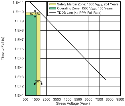
| TA upto 150°C | Operating lifetime = 135 years | |
| Stress-voltage frequency = 60 Hz | ||
| Isolation working voltage = 1500 VRMS | ||
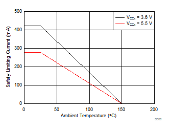 Figure 3. Thermal Derating Curve for Limiting Current for DW Package
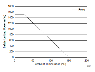 Figure 5. Thermal Derating Curve for Limiting Power for DW Package
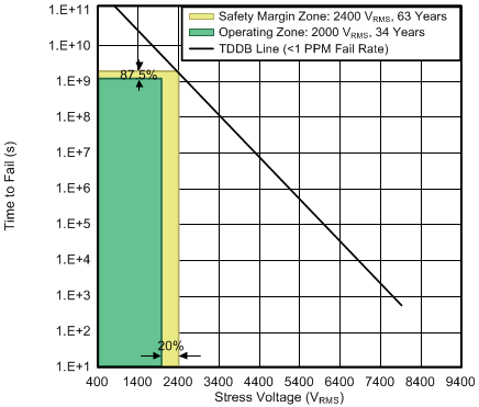
| TA upto 150°C | Operating lifetime = 34 years | |
| Stress-voltage frequency = 60 Hz | ||
| Isolation working voltage = 2000 VRMS | ||
 Figure 4. Thermal Derating Curve for Limiting Current for DWW Package
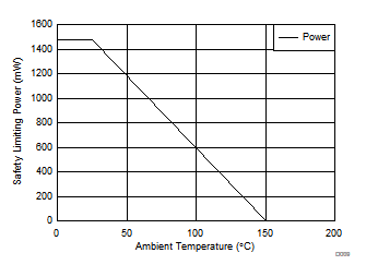 Figure 6. Thermal Derating Curve for Limiting Power for DWW Package
6.14 Typical Characteristics
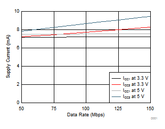
| TA = 25°C | CH-A toggle |
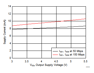
| TA = 25°C |
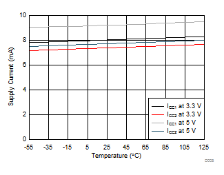
| Data rate = 150 Mbps | CH-B toggle |
| TA = 25°C |
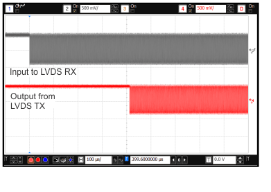 Figure 15. Distortion Correction Scheme Calibration Time (tCALIB)
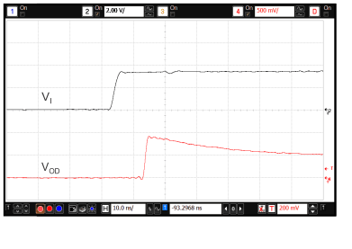 Figure 17. Disable to Enable Time (tPZH)
| TA = 25°C | CH-B toggle |
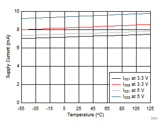
| Data rate = 150 Mbps | CH-A toggle |
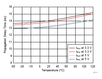
| TA = 25°C |
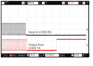 Figure 16. Transition From Valid Data to Idle (tIDLE_OUT)
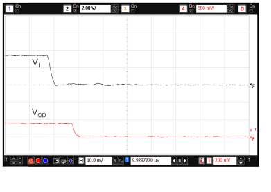 Figure 18. Disable Time (tPLZ, tPHZ)