ZHCSFH9 September 2016 ADS9120
PRODUCTION DATA.
- 1 特性
- 2 应用
- 3 说明
- 4 修订历史记录
- 5 Pin Configuration and Functions
-
6 Specifications
- 6.1 Absolute Maximum Ratings
- 6.2 ESD Ratings
- 6.3 Recommended Operating Conditions
- 6.4 Thermal Information
- 6.5 Electrical Characteristics
- 6.6 Timing Requirements: Conversion Cycle
- 6.7 Timing Requirements: Asynchronous Reset, NAP, and PD
- 6.8 Timing Requirements: SPI-Compatible Serial Interface
- 6.9 Timing Requirements: Source-Synchronous Serial Interface (External Clock)
- 6.10 Timing Requirements: Source-Synchronous Serial Interface (Internal Clock)
- 6.11 Typical Characteristics
-
7 Detailed Description
- 7.1 Overview
- 7.2 Functional Block Diagram
- 7.3 Feature Description
- 7.4 Device Functional Modes
- 7.5
Programming
- 7.5.1 Data Transfer Frame
- 7.5.2 Interleaving Conversion Cycles and Data Transfer Frames
- 7.5.3 Data Transfer Protocols
- 7.5.4 Device Setup
- 7.6 Register Maps
- 8 Application and Implementation
- 9 Power-Supply Recommendations
- 10Layout
- 11器件和文档支持
- 12机械、封装和可订购信息
10 Layout
10.1 Layout Guidelines
This section provides some recommended layout guidelines for achieving optimum performance with the ADS9120 device.
10.1.1 Signal Path
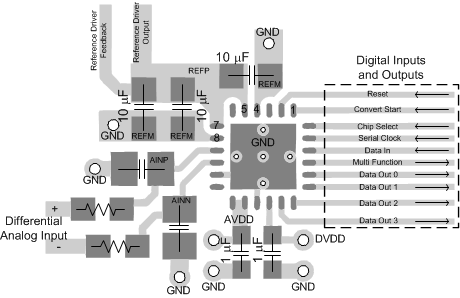
As illustrated in Figure 100, the analog input and reference signals are routed in opposite directions to the digital connections. This arrangement prevents noise generated by digital switching activity from coupling to sensitive analog signals.
10.1.2 Grounding and PCB Stack-Up
Low inductance grounding is critical for achieving optimum performance. Grounding inductance is kept below 1 nH with 15-mil grounding vias and a printed circuit board (PCB) layout design that has at least four layers. Place all critical components of the signal chain on the top layer with a solid analog ground from subsequent inner layers to minimize via length to ground.
Pins 11 and 15 of the ADS9120 can be easily grounded with very low inductance by placing at least four 8-mil grounding vias at the ADS9120 thermal pad. Afterwards, pins 11 and 15 can be connected directly to the grounded thermal path.
10.1.3 Decoupling of Power Supplies
Place the AVDD and DVDD supply decoupling capacitors within 20 mil from the supply pins and use a 15-mil via to ground from each capacitor. Avoid placing vias between any supply pin and its decoupling capacitor.
10.1.4 Reference Decoupling
Dynamic currents are also present at the REFP and REFM pins during the conversion phase and excellent decoupling is required to achieve optimum performance. Three 10-μF, X7R-grade, ceramic capacitors with 10-V rating are recommended, placed as illustrated in Figure 100. Select 0603- or 0805-size capacitors to keep ESL low. The REFM pin of each pair must be connected to the decoupling capacitor before a ground via.
10.1.5 Differential Input Decoupling
Dynamic currents are also present at the differential analog inputs of the ADS9120. C0G- or NPO-type capacitors are required to decouple these inputs because their capacitance stays almost constant over the full input voltage range. Lower quality capacitors (such as X5R and X7R) have large capacitance changes over the full input voltage range that can cause degradation in the performance of the ADS9120.
10.2 Layout Example
 Figure 100. Recommended Layout