ZHCSFJ0B August 2016 – February 2017 LM27762
PRODUCTION DATA.
- 1 特性
- 2 应用
- 3 说明
- 4 修订历史记录
- 5 Pin Configuration and Functions
- 6 Specifications
- 7 Detailed Description
-
8 Application and Implementation
- 8.1 Application Information
- 8.2
Typical Application
- 8.2.1 Design Requirements
- 8.2.2 Detailed Design Procedure
- 8.2.3 Application Curves
- 9 Power Supply Recommendations
- 10Layout
- 11器件和文档支持
- 12机械、封装和可订购信息
10 Layout
10.1 Layout Guidelines
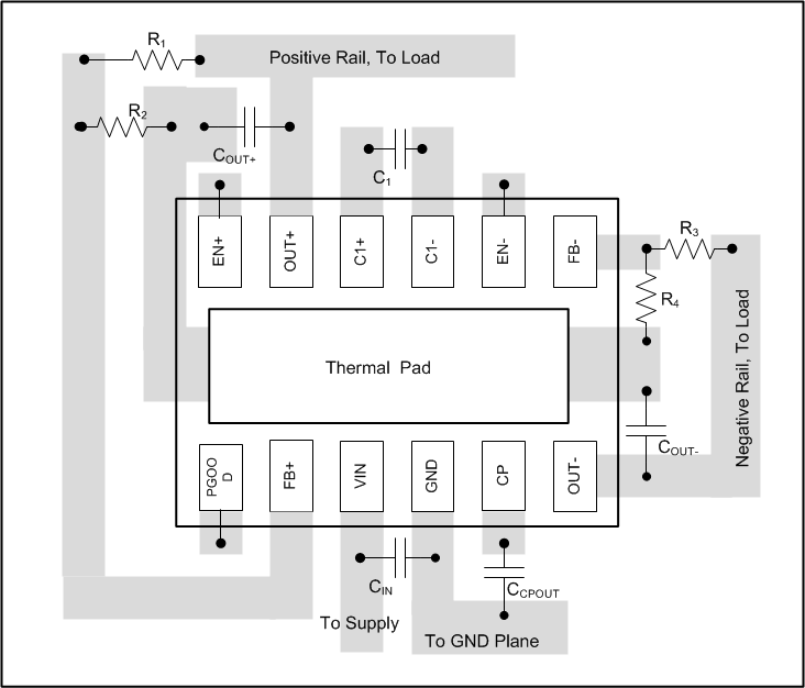
The high switching frequency and large switching currents of the LM27762 make the choice of layout important. Use the following steps as a reference to ensure the device is stable and maintains proper LED current regulation across its intended operating voltage and current range:
- Place CIN on the top layer (same layer as the LM27762) and as close as possible to the device. Connecting the input capacitor through short, wide traces to both the VIN and GND pins reduces the inductive voltage spikes that occur during switching, which can corrupt the VIN line.
- Place CCPOUT on the top layer (same layer as the LM27762) and as close as possible to the VOUT and GND pins. The returns for both CIN and CCPOUT must come together at one point, as close as possible to the GND pin. Connecting CCPOUT through short, wide traces reduces the series inductance on the VCPOUT and GND pins that can corrupt the VCPOUT and GND lines and cause excessive noise in the device and surrounding circuitry.
- Place C1 on top layer (same layer as the LM27762) and as close as possible to the device. Connect the flying capacitor through short, wide traces to both the C1+ and C1– pins.
- Place COUT+, COUT– on the top layer (same layer as the LM27762) and as close to the respective OUT pin as possible. For best performance the ground connection for COUT must connect back to the GND connection at the thermal pad of the device.
- Place R1 to R4 on the top layer (same layer as LM27762) and as close as possible to the respective FB pin. For best performance the ground connection of R2, R4 must connect back to the GND connection at the thermal pad of the device.
Connections using long trace lengths, narrow trace widths, or connections through vias must be avoided. These add parasitic inductance and resistance that results in inferior performance, especially during transient conditions.
10.2 Layout Example
 Figure 16. LM27762 Layout Example
(Note: Pullup resistor for PGOOD not shown in example.)