ZHCSFJ0B August 2016 – February 2017 LM27762
PRODUCTION DATA.
- 1 特性
- 2 应用
- 3 说明
- 4 修订历史记录
- 5 Pin Configuration and Functions
- 6 Specifications
- 7 Detailed Description
-
8 Application and Implementation
- 8.1 Application Information
- 8.2
Typical Application
- 8.2.1 Design Requirements
- 8.2.2 Detailed Design Procedure
- 8.2.3 Application Curves
- 9 Power Supply Recommendations
- 10Layout
- 11器件和文档支持
- 12机械、封装和可订购信息
6 Specifications
6.1 Absolute Maximum Ratings
over operating free-air temperature range (unless otherwise noted)(1)(2)| MIN | MAX | UNIT | ||
|---|---|---|---|---|
| VIN to GND or GND to VOUT | 5.8 | V | ||
| EN+, EN- | GND − 0.3 | VIN | V | |
| CPOUT, OUT+ and OUT- , continuous output current | 300 | mA | ||
| OUT+, OUT- short-circuit duration to GND(3) | 1 | s | ||
| Continuous power dissipation(4) | Internally limited | |||
| TJMAX(4) | 150 | °C | ||
| Operating input voltage, VIN | 2.7 | 5.5 | V | |
| Operating output current, IOUT | 0 | 250 | mA | |
| Operating ambient temperature, TA | –40 | 85 | °C | |
| Operating junction temperature, TJ | –40 | 125 | °C | |
| Storage temperature, Tstg | –65 | 150 | °C | |
(1) Stresses beyond those listed under Absolute Maximum Ratings may cause permanent damage to the device. These are stress ratings only, which do not imply functional operation of the device at these or any other conditions beyond those indicated under Recommended Operating Conditions. Exposure to absolute-maximum-rated conditions for extended periods may affect device reliability.
(2) If Military/Aerospace specified devices are required, contact the TI Sales Office/Distributors for availability and specifications.
(3) OUT may be shorted to GND for one second without damage. However, shorting OUT to VIN may damage the device and must be avoided. Also, for temperatures above TA = 85°C, VOUT must not be shorted to GND or VIN or device may be damaged.
(4) Internal thermal shutdown circuitry protects the device from damage.
6.2 ESD Ratings
| VALUE | UNIT | |||
|---|---|---|---|---|
| V(ESD) | Electrostatic discharge | Human-body model (HBM), per ANSI/ESDA/JEDEC JS-001(1) | ±1000 | V |
| Charged-device model (CDM), per JEDEC specification JESD22-C101(2) | ±250 | |||
(1) JEDEC document JEP155 states that 500-V HBM allows safe manufacturing with a standard ESD control process.
(2) JEDEC document JEP157 states that 250-V CDM allows safe manufacturing with a standard ESD control process.
6.3 Recommended Operating Conditions
over operating free-air temperature range (unless otherwise noted)| MIN | MAX | UNIT | ||
|---|---|---|---|---|
| Operating ambient temperature, TA | –40 | 85 | °C | |
| Operating junction temperature, TJ | –40 | 125 | °C | |
6.4 Thermal Information
| THERMAL METRIC(1) | LM27762 | UNIT | |
|---|---|---|---|
| DSS (WSON) | |||
| 12 PINS | |||
| RθJA | Junction-to-ambient thermal resistance | 62.2 | °C/W |
| RθJC(top) | Junction-to-case (top) thermal resistance | 54.7 | °C/W |
| RθJB | Junction-to-board thermal resistance | 25.6 | °C/W |
| ψJT | Junction-to-top characterization parameter | 1.8 | °C/W |
| ψJB | Junction-to-board characterization parameter | 25.6 | °C/W |
| RθJC(bot) | Junction-to-case (bottom) thermal resistance | 9.2 | °C/W |
(1) For more information about traditional and new thermal metrics, see Semiconductor and IC Package Thermal Metrics.
6.5 Electrical Characteristics
Typical limits apply for TA = 25°C; minimum and maximum limits apply over the full temperature range. Unless otherwise specified VIN = 5 V, CIN = COUT+ = COUT– = 2.2 μF, C1 = 1 μF, CPOUT = 4.7 μF.| PARAMETER | TEST CONDITIONS | MIN | TYP | MAX | UNIT | |
|---|---|---|---|---|---|---|
| IQ | Supply current | Open circuit, no load, EN+, EN– connected to VIN. (1) | 390 | µA | ||
| ISD | Shutdown supply current | 0.5 | 5 | µA | ||
| ƒSW | Switching frequency | VIN = 3.6 V | 1.7 | 2 | 2.3 | MHz |
| RNEG | Output resistance to CPOUT | VIN = 5.5 V, IL = 100 mA | 2.5 | Ω | ||
| VLDO– | LDO dropout voltage | IL = 100 mA, VOUT– = −5 V | 30 | mV | ||
| PSRR | Power supply rejection ratio, OUT– | IL = 100 mA, VOUT– = −1.8 V, 10 kHz | 50 | dB | ||
| VN– | Output noise voltage | IL = 80 mA, 10 Hz to 100 kHz | 22 | µVRMS | ||
| VFB– | Feedback pin reference voltage | –1.238 | –1.22 | –1.202 | V | |
| VOUT– | Adjustable output voltage | 5.5 V ≥ VIN ≥ 2.7 V | –5 | –1.5 | V | |
| Load regulation | 0 to 250 mA, VOUT = –1.8 V | 34 | µV/mA | |||
| Line regulation | 5 V ≥ VIN ≥ 2.7 V, IL = 50 mA | 1.5 | mV/V | |||
| VLDO+ | LDO dropout voltage | IL = 100 mA, VOUT = 5 V | 45 | mV | ||
| PSRR | Power supply rejection ratio, OUT+ | IL = 100 mA, VOUT+ = 1.8 V, 10 kHz | 43 | dB | ||
| VN+ | Output noise voltage | IL = 80 mA, 10 Hz to 100 kHz | 22 | µVRMS | ||
| VFB+ | Feedback pin reference voltage | 1.182 | 1.2 | 1.218 | V | |
| VOUT+ | Adjustable output voltage | 5.5 V ≥ VIN ≥ 2.7 V | 1.5 | 5 | V | |
| Load regulation | 0 to 250 mA, VOUT = 1.8 V | 11 | µV/mA | |||
| Line regulation | 5 V ≥ VIN ≥ 2.7 V, IL = 50 mA | 1.9 | mV/V | |||
| VIH | Enable pin input voltage high | 5.5 V ≥ VIN ≥ 2.7 V | 1.2 | V | ||
| VIL | Enable pin input voltage low | 5.5 V ≥ VIN ≥ 2.7 V | 0.4 | V | ||
(1) When VIN = 5.5V charge pump may enter PWM mode in hot conditions.
6.6 Typical Characteristics
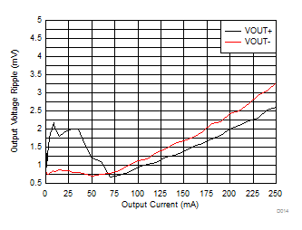
| VIN = 3.7 V | VOUT = ±3 V | |
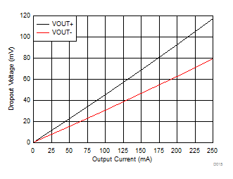
| VOUT = ± 3.3 V | ||
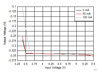
| VOUT = –3.3 V | ||
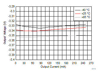
| VIN = 4.3 V | VOUT = –3.3 V | |
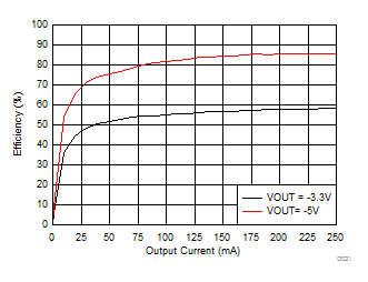
| VIN = 5.5 V | ||
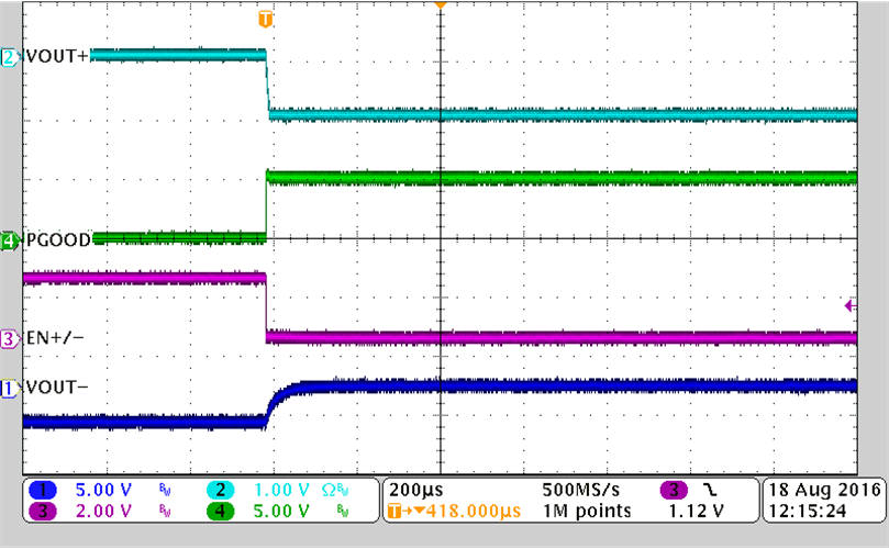
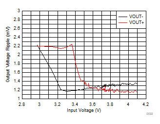
| VOUT = ±3 V | IOUT = ±100 mA | |
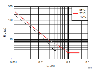
| VIN = 5.5 V | ||
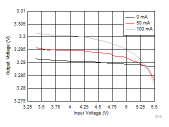
| VOUT = 3.3 V | ||
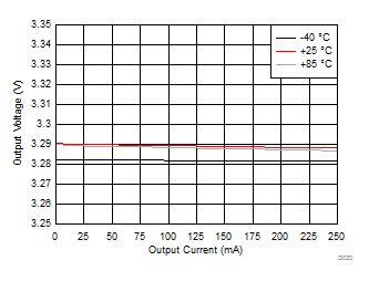
| VIN = 4.3 V | VOUT = 3.3 V | |
