ZHCSFJ8 September 2016 ISO5451-Q1
PRODUCTION DATA.
- 1 特性
- 2 应用
- 3 说明
- 4 修订历史记录
- 5 说明 (续)
- 6 Pin Configuration and Function
-
7 Specifications
- 7.1 Absolute Maximum Ratings
- 7.2 ESD Ratings
- 7.3 Recommended Operating Conditions
- 7.4 Thermal Information
- 7.5 Power Rating
- 7.6 Insulation Characteristics
- 7.7 Safety Limiting Values
- 7.8 Safety-Related Certifications
- 7.9 Electrical Characteristics
- 7.10 Switching Characteristics
- 7.11 Safety and Insulation Characteristics Curves
- 7.12 Typical Characteristics
- 8 Parameter Measurement Information
- 9 Detailed Description
-
10Application and Implementation
- 10.1 Application Information
- 10.2
Typical Applications
- 10.2.1 Design Requirements
- 10.2.2
Detailed Design Procedure
- 10.2.2.1 Recommended ISO5451-Q1 Application Circuit
- 10.2.2.2 FLT and RDY Pin Circuitry
- 10.2.2.3 Driving the Control Inputs
- 10.2.2.4 Local Shutdown and Reset
- 10.2.2.5 Global-Shutdown and Reset
- 10.2.2.6 Auto-Reset
- 10.2.2.7 DESAT Pin Protection
- 10.2.2.8 DESAT Diode and DESAT Threshold
- 10.2.2.9 Determining the Maximum Available, Dynamic Output Power, POD-max
- 10.2.2.10 Example
- 10.2.2.11 Higher Output Current Using an External Current Buffer
- 10.2.3 Application Curve
- 11Power Supply Recommendations
- 12Layout
- 13器件和文档支持
- 14机械、封装和可订购信息
7 Specifications
7.1 Absolute Maximum Ratings(1)
over operating free-air temperature range (unless otherwise noted)| MIN | MAX | UNIT | ||||
|---|---|---|---|---|---|---|
| VCC1 | Supply voltage input side | GND1 - 0.3 | 6 | V | ||
| VCC2 | Positive supply voltage output side | (VCC2 – GND2) | –0.3 | 35 | V | |
| VEE2 | Negative supply voltage output side | (VEE2 – GND2) | –17.5 | 0.3 | V | |
| V(SUP2) | Total supply output voltage | (VCC2 - VEE2) | –0.3 | 35 | V | |
| VOUT | Gate driver output voltage | VEE2 - 0.3 | VCC2 + 0.3 | V | ||
| I(OUTH) | Gate driver high output current | Gate driver high output current (max pulse width = 10 μs, max duty cycle = 0.2%) |
2.7 | A | ||
| I(OUTL) | Gate driver low output current | 5.5 | A | |||
| V(LIP) | Voltage at IN+, IN-, FLT, RDY, RST | GND1 - 0.3 | VCC1 + 0.3 | V | ||
| I(LOP) | Output current of FLT, RDY | 10 | mA | |||
| V(DESAT) | Voltage at DESAT | GND2 - 0.3 | VCC2 + 0.3 | V | ||
| V(CLAMP) | Clamp voltage | VEE2 - 0.3 | VCC2 + 0.3 | V | ||
| TJ | Junction temperature | –40 | 150 | °C | ||
| TSTG | Storage temperature | -65 | 150 | °C | ||
(1) Stresses beyond those listed under absolute maximum ratings may cause permanent damage to the device. These are stress ratings only and functional operation of the device at these or any conditions beyond those indicated under recommended operating conditions is not implied. Exposure to absolute-maximum-rated conditions for extended periods may affect device reliability
7.2 ESD Ratings
| VALUE | UNIT | |||
|---|---|---|---|---|
| V(ESD) | Electrostatic discharge | Human-body model (HBM), per AEC Q100-002(1) | ±4000 | V |
| Charged-device model (CDM), per AEC Q100-011 | ±1500 | |||
(1) AEC Q100-002 indicates that HBM stressing shall be in accordance with the ANSI/ESDA/JEDEC JS-001 specification.
7.3 Recommended Operating Conditions
over operating free-air temperature range (unless otherwise noted)| MIN | NOM | MAX | UNIT | ||
|---|---|---|---|---|---|
| VCC1 | Supply voltage input side | 3 | 5.5 | V | |
| VCC2 | Positive supply voltage output side (VCC2 – GND2) | 15 | 30 | V | |
| VEE2 | Negative supply voltage output side (VEE2 – GND2) | –15 | 0 | V | |
| V(SUP2) | Total supply voltage output side (VCC2 – VEE2) | 15 | 30 | V | |
| VIH | High-level input voltage (IN+, IN-, RST) | 0.7 x VCC1 | VCC1 | V | |
| VIL | Low-level input voltage (IN+, IN-, RST) | 0 | 0.3 x VCC1 | V | |
| tUI | Pulse width at IN+, IN- for full output (CLOAD = 1nF) | 40 | ns | ||
| tRST | Pulse width at RST for resetting fault latch | 800 | ns | ||
| TA | Ambient temperature | -40 | 25 | 125 | °C |
7.4 Thermal Information
| THERMAL METRIC(1) | DW (SOIC) | UNIT | |
|---|---|---|---|
| 16 PINS | |||
| RθJA | Junction-to-ambient thermal resistance | 99.6 | °C/W |
| RθJC(top) | Junction-to-case (top) thermal resistance | 48.5 | |
| RθJB | Junction-to-board thermal resistance | 56.5 | |
| ψJT | Junction-to-top characterization parameter | 29.2 | |
| ψJB | Junction-to-board characterization parameter | 56.5 | |
(1) For more information about traditional and new thermal metrics, see the Semiconductor and IC Package Thermal Metrics application report.
7.5 Power Rating
| VALUE | UNIT | |||
|---|---|---|---|---|
| PD | Maximum power dissipation(1) | 1255 | mW | |
| PID | Maximum input power dissipation | 175 | ||
| POD | Maximum output power dissipation | 1080 | ||
(1) Full chip power dissipation is de-rated 10.04 mW/°C beyond 25°C ambient temperature. At 125°C ambient temperature, a maximum of 251 mW total power dissipation is allowed. Power dissipation can be optimized depending on ambient temperature and board design, while ensuring that Junction temperature does not exceed 150°C.
7.6 Insulation Characteristics
| PARAMETER | TEST CONDITIONS | SPECIFICATION | UNIT | |
|---|---|---|---|---|
| CLR | External clearance(1) | Shortest terminal-to-terminal distance through air | >8 | mm |
| CPG | External creepage(1) | Shortest terminal-to-terminal distance across the package surface | >8 | mm |
| DTI | Distance through the insulation | Minimum internal gap (internal clearance) | >21 | μm |
| CTI | Tracking resistance (comparative tracking index) | DIN EN 60112 (VDE 0303-11); IEC 60112; | >600 | V |
| Material Group | According to IEC 60664-1; UL 746A | I | ||
| Overvoltage category (according to IEC 60664-1) | Rated Mains Voltage ≤ 300 VRMS | I-IV | ||
| Rated Mains Voltage ≤ 600 VRMS | I-III | |||
| Rated Mains Voltage ≤ 1000 VRMS | I-II | |||
| DIN V VDE V 0884-10 (VDE V 0884-10):2006-12(2) | ||||
| VIORM | Maximum repetitive peak isolation voltage | AC voltage (bipolar) | 1420 | VPK |
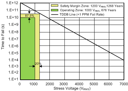
| VIOWM | Maximum isolation working voltage | AC voltage. Time dependent dielectric breakdown (TDDB) Test, see Figure 1 | 1000 | VRMS |
| DC voltage | 1420 | VDC | ||
| VIOTM | Maximum Transient isolation voltage | VTEST = VIOTM, t = 60 sec (qualification), t = 1 sec (100% production) | 8000 | VPK |
| VIOSM | Maximum surge isolation voltage(3) | Test method per IEC 60065, 1.2/50 μs waveform, VTEST = 1.6 x VIOSM = 10000 VPK (qualification)(3) |
6250 | |
| qpd | Apparent charge(4) | Method a: After I/O safety test subgroup 2/3, Vini = VIOTM, tini = 60 s; Vpd(m) = 1.2 × VIORM = 1704 VPK , tm = 10 s |
≤5 | pC |
| Method a: After environmental tests subgroup 1, Vini = VIOTM, tini = 60 s; Vpd(m) = 1.6 × VIORM = 2272 VPK , tm = 10 s |
≤5 | |||
| Method b1: At routine test (100% production) and preconditioning (type test) Vini = VIOTM, tini = 60 s; Vpd(m) = 1.875× VIORM = 2663 VPK , tm = 10 s |
≤5 | |||
| RIO | Isolation resistance, input to output(5) | VIO = 500 V, TA = 25°C | > 1012 | Ω |
| VIO = 500 V, 100°C ≤ TA ≤ 125°C | > 1011 | Ω | ||
| VIO = 500 V at TS = 150°C | > 109 | Ω | ||
| CIO | Barrier capacitance, input to output(5) | VIO = 0.4 x sin (2πft), f = 1 MHz | 1 | pF |
| Pollution degree | 2 | |||
| UL 1577 | ||||
| VISO | Withstanding Isolation voltage | VTEST = VISO, t = 60 sec (qualification), VTEST = 1.2 × VISO = 6840 VRMS, t = 1 sec (100% production) |
5700 | VRMS |
(1) Creepage and clearance requirements should be applied according to the specific equipment isolation standards of an application. Care should be taken to maintain the creepage and clearance distance of a board design to ensure that the mounting pads of the isolator on the printed-circuit board do not reduce this distance. Creepage and clearance on a printed-circuit board become equal in certain cases. Techniques such as inserting grooves and/or ribs on a printed circuit board are used to help increase these specifications.
(2) This coupler is suitable for basic electrical insulation only within the maximum operating ratings. Compliance with the safety ratings shall be ensured by means of suitable protective circuits.
(3) Testing is carried out in air or oil to determine the intrinsic surge immunity of the isolation barrier.
(4) Apparent charge is electrical discharge caused by a partial discharge (pd).
(5) All pins on each side of the barrier tied together creating a two-terminal device
7.7 Safety Limiting Values
Safety limiting intends to prevent potential damage to the isolation barrier upon failure of input or output circuitry. A failure of the I/O can allow low resistance to ground or the supply and, without current limiting, dissipate sufficient power to overheat the die and damage the isolation barrier, potentially leading to secondary system failures.| PARAMETER | TEST CONDITIONS | MIN | TYP | MAX | UNIT | ||
|---|---|---|---|---|---|---|---|
| IS | Safety input, output or supply current | θJA = 99.6°C/W, VI = 3.6 V, TJ = 150°C, TA = 25°C |
349 | mA | |||
| θJA = 99.6°C/W, VI = 5.5 V, TJ = 150°C, TA = 25°C |
228 | ||||||
| θJA = 99.6°C/W, VI = 15 V, TJ = 150°C, TA = 25°C |
84 | ||||||
| θJA = 99.6°C/W, VI = 30 V, TJ = 150°C, TA = 25°C |
42 | ||||||
| PS | Safety input, output, or total power | θJA = 99.6°C/W, TJ = 150°C, TA = 25°C | 1255(1) | ||||
| TS | Maximum ambient safety temperature | 150 | °C | ||||
(1) Input, output, or the sum of input and output power should not exceed this value
7.8 Safety-Related Certifications
over operating free-air temperature range (unless otherwise noted)| VDE | CSA | UL | CQC | TUV |
|---|---|---|---|---|
| Certified according to DIN V VDE V 0884-10 (VDE V 0884-10):2006-12 and DIN EN 60950-1 (VDE 0805 Teil 1):2011-01 |
Plan to certify under CSA Component Acceptance Notice 5A, IEC 60950-1 and IEC 60601-1 | Certified according to UL 1577 Component Recognition Program | Certified according to GB 4943.1-2011 | Certified according to EN 61010-1:2010 (3rd Ed) and EN 60950-1:2006/A11:2009/A1:2010/ A12:2011/A2:2013 |
| Reinforced Insulation Maximum Transient isolation voltage, 8000 VPK; Maximum surge isolation voltage, 6250 VPK, Maximum repetitive peak isolation voltage, 1420 VPK |
Isolation Rating of 5700 VRMS; Reinforced insulation per CSA 60950- 1- 07+A1+A2 and IEC 60950-1 (2nd Ed.), 800 VRMS max working voltage (pollution degree 2, material group I) ; 2 MOPP (Means of Patient Protection) per CSA 60601-1:14 and IEC 60601-1 Ed. 3.1, 250 VRMS (354 VPK) max working voltage |
Single Protection, 5700 VRMS (1) | Reinforced Insulation, Altitude ≤ 5000m, Tropical climate, 400 VRMS maximum working voltage | 5700 VRMS Reinforced insulation per EN 61010-1:2010 (3rd Ed) up to working voltage of 600 VRMS 5700 VRMS Reinforced insulation per EN 60950-1:2006/A11:2009/A1:2010/ A12:2011/A2:2013 up to working voltage of 800 VRMS |
| Certification completed Certificate number: 40040142 |
Certification planned | Certification completed File number: E181974 |
Certification completed Certificate number: CQC16001141761 |
Certification completed Client ID number: 77311 |
(1) Production tested ≥ 6840 VRMS for 1 second in accordance with UL 1577.
The safety-limiting constraint is the absolute-maximum junction temperature specified in the Absolute Maximum Ratings table. The power dissipation and junction-to-air thermal impedance of the device installed in the application hardware determines the junction temperature. The assumed junction-to-air thermal resistance in the Thermal Information table is that of a device installed in the High-K Test Board for Leaded Surface-Mount Packages. The power is the recommended maximum input voltage times the current. The junction temperature is then the ambient temperature plus the power times the junction-to-air thermal resistance.
7.9 Electrical Characteristics
Over recommended operating conditions unless otherwise noted. All typical values are at TA = 25°C, VCC1 = 5 V,VCC2 – GND2 = 15 V, GND2 – VEE2 = 8 V
| PARAMETER | TEST CONDITIONS | MIN | TYP | MAX | UNIT | ||
|---|---|---|---|---|---|---|---|
| VOLTAGE SUPPLY | |||||||
| VIT+(UVLO1) | Positive-going UVLO1 threshold voltage input side (VCC1 – GND1) | 2.25 | V | ||||
| VIT-(UVLO1) | Negative-going UVLO1 threshold voltage input side (VCC1 – GND1) | 1.7 | V | ||||
| VHYS(UVLO1) | UVLO1 Hysteresis voltage (VIT+ – VIT–) input side | 0.24 | V | ||||
| VIT+(UVLO2) | Positive-going UVLO2 threshold voltage output side (VCC2 – GND2) | 12 | 13 | V | |||
| VIT-(UVLO2) | Negative-going UVLO2 threshold voltage output side (VCC2 – GND2) | 9.5 | 11 | V | |||
| VHYS(UVLO2) | UVLO2 Hysteresis voltage (VIT+ – VIT–) output side | 1 | V | ||||
| IQ1 | Input supply quiescent current | 2.8 | 4.5 | mA | |||
| IQ2 | Output supply quiescent current | 3.6 | 6 | mA | |||
| LOGIC I/O | |||||||
| VIT+(IN,RST) | Positive-going input threshold voltage (IN+, IN-, RST) | 0.7 x VCC1 | V | ||||
| VIT-(IN,RST) | Negative-going input threshold voltage (IN+, IN-, RST) | 0.3 x VCC1 | V | ||||
| VHYS(IN,RST) | Input hysteresis voltage (IN+, IN-, RST) | 0.15 x VCC1 | V | ||||
| IIH | High-level input leakage at (IN+) (1) | IN+ = VCC1 | 100 | µA | |||
| IIL | Low-level input leakage at (IN-, RST) (2) | IN- = GND1, RST = GND1 | -100 | µA | |||
| IPU | Pull-up current of FLT, RDY | V(RDY) = GND1, V(FLT) = GND1 | 100 | µA | |||
| VOL | Low-level output voltage at FLT, RDY | I(FLT) = 5 mA | 0.2 | V | |||
| GATE DRIVER STAGE | |||||||
| V(OUTPD) | Active output pull-down voltage | IOUT = 200 mA, VCC2 = open | 2 | V | |||
| V(OUTH) | High-level output voltage | IOUT = –20 mA | VCC2 - 0.5 | VCC2 - 0.24 | V | ||
| V(OUTL) | Low-level output voltage | IOUT = 20 mA | VEE2 + 13 | VEE2 + 50 | mV | ||
| I(OUTH) | High-level output peak current | IN+ = high, IN- = low, VOUT = VCC2 - 15 V |
1.5 | 2.5 | A | ||
| I(OUTL) | Low-level output peak current | IN+ = low, IN- = high, VOUT = VEE2 + 15 V |
3.4 | 5 | A | ||
| ACTIVE MILLER CLAMP | |||||||
| V(CLP) | Low-level clamp voltage | I(CLP) = 20 mA | VEE2 + 0.015 | VEE2 + 0.08 | V | ||
| I(CLP) | Low-level clamp current | V(CLAMP) = VEE2 + 2.5 V | 1.6 | 2.5 | A | ||
| V(CLTH) | Clamp threshold voltage | 1.6 | 2.1 | 2.5 | V | ||
| SHORT CIRCUIT CLAMPING | |||||||
| V(CLP_OUT) | Clamping voltage (VOUT - VCC2) |
IN+ = high, IN- = low, tCLP=10 µs, I(OUTH) = 500 mA | 0.8 | 1.3 | V | ||
| V(CLP_CLAMP) | Clamping voltage (VCLP - VCC2) |
IN+ = high, IN- = low, tCLP=10 µs, I(CLP) = 500 mA | 1.3 | V | |||
| V(CLP_CLAMP) | Clamping voltage at CLAMP | IN+ = High, IN- = Low, I(CLP) = 20 mA | 0.7 | 1.1 | V | ||
| DESAT PROTECTION | |||||||
| I(CHG) | Blanking capacitor charge current | V(DESAT) - GND2 = 2 V | 0.42 | 0.5 | 0.58 | mA | |
| I(DCHG) | Blanking capacitor discharge current | V(DESAT) - GND2 = 6 V | 9 | 14 | mA | ||
| V(DSTH) | DESAT threshold voltage with respect to GND2 | 8.3 | 9 | 9.5 | V | ||
| V(DSL) | DESAT voltage with respect to GND2, when OUT is driven low | 0.4 | 1 | V | |||
(1) IIH for IN-, RST pin is zero as they are pulled high internally.
(2) IIL for IN+ is zero, as it is pulled low internally.
7.10 Switching Characteristics
Over recommended operating conditions unless otherwise noted. All typical values are at TA = 25°C, VCC1 = 5 V,VCC2 – GND2 = 15 V, GND2 – VEE2 = 8 V
| PARAMETER | TEST CONDITIONS | MIN | TYP | MAX | UNIT | |
|---|---|---|---|---|---|---|
| tr | Output signal rise time | CLOAD = 1 nF, see Figure 38, Figure 39 and Figure 40 | 12 | 20 | 35 | ns |
| tf | Output signal fall time | 12 | 20 | 37 | ns | |
| tPLH, tPHL | Propagation Delay | 76 | 110 | ns | ||
| tsk-p | Pulse Skew |tPHL – tPLH| | 20 | ns | |||
| tsk-pp | Part-to-part skew | 30(1) | ns | |||
| tGF | Glitch filter on IN+, IN-, RST | 20 | 30 | 40 | ns | |
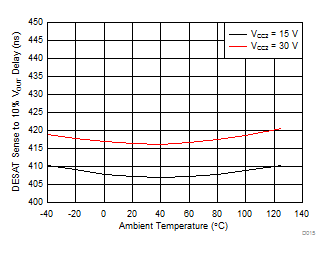
| tDESAT (10%) | DESAT sense to 10% OUT delay | 300 | 415 | 500 | ns | |
| tDESAT (GF) | DESAT glitch filter delay | 330 | ns | |||
| tDESAT (FLT) | DESAT sense to FLT-low delay | see Figure 40 | 2000 | 2420 | ns | |
| tLEB | Leading edge blanking time | see Figure 38 and Figure 39 | 330 | 400 | 500 | ns |
| tGF(RSTFLT) | Glitch filter on RST for resetting FLT | 300 | 800 | ns | ||
| CI | Input capacitance(2) | VI = VCC1/2 + 0.4 x sin (2πft), f = 1 MHz, VCC1 = 5 V |
2 | pF | ||
| CMTI | Common-mode transient immunity | VCM = 1500 V, see Figure 41 | 50 | 100 | kV/μs | |
(1) Measured at same supply voltage and temperature condition
(2) Measured from input pin to ground.
7.11 Safety and Insulation Characteristics Curves
| TA upto 150°C | Stress-voltage frequency = 60 Hz | |||
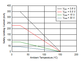 Figure 2. Thermal Derating Curve for Safety Limiting Current per VDE
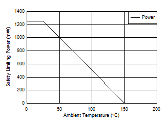 Figure 3. Thermal Derating Curve for Safety Limiting Power per VDE
7.12 Typical Characteristics
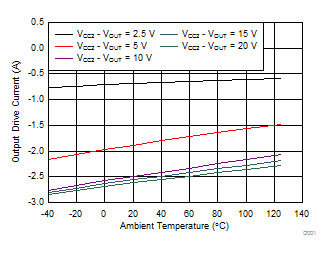
| VCC2 = 30 V |
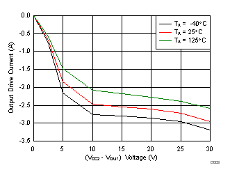
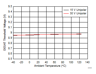
| Unipolar: VCC2 - VEE2 = VCC2 - GND2 | ||
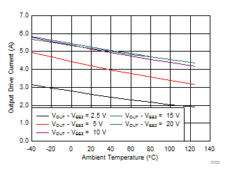
| VCC2 = 30 V |
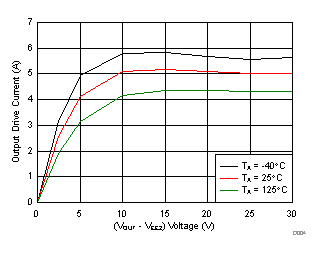
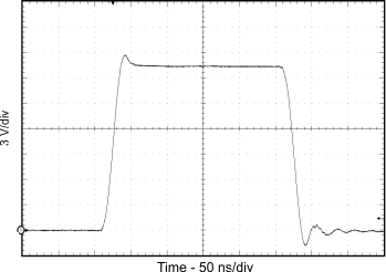
| CL = 1 nF | RG = 0 Ω | |
| VCC2 - VEE2 = VCC2 - GND2 = 20 V | ||
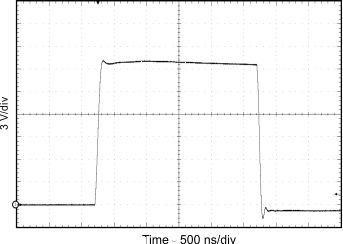
| CL = 10 nF | RG = 0 Ω | |
| VCC2 - VEE2 = VCC2 - GND2 = 20 V | ||
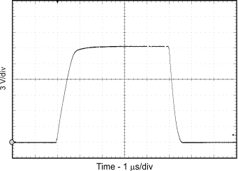
| CL = 100 nF | RG = 0 Ω | |
| VCC2 - VEE2 = VCC2 - GND2 = 20 V | ||
| CL = 100 nF | RG = 10 Ω | |
| VCC2 - VEE2 = VCC2 - GND2 = 20 V | ||
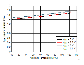
| IN+ = Low | IN- = Low |
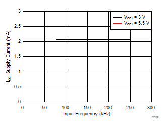
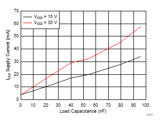
| RG = 10 Ω, 20kHz |
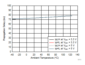
| CL = 1nF | RG = 0 Ω | VCC2 = 15 V |
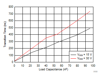
| RG = 0 Ω | VCC1 = 5 V |
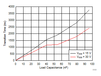
| RG = 10 Ω | VCC1 = 5 V |
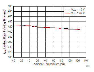
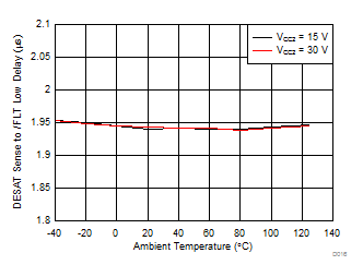
| CL = 1 nF |
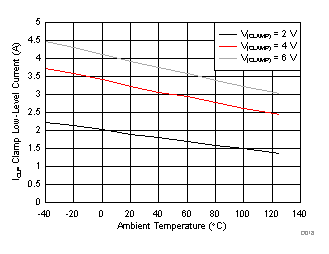
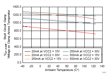
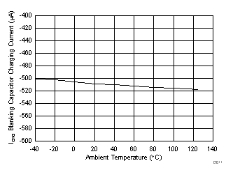
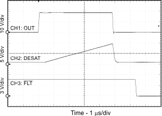
| VCC2 = 15 V | DESAT = 6 V |
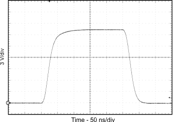
| CL = 1 nF | RG = 10 Ω | |
| VCC2 - VEE2 = VCC2 - GND2 = 20 V | ||
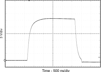
| CL = 10 nF | RG = 10 Ω | |
| VCC2 - VEE2 = VCC2 - GND2 = 20 V | ||
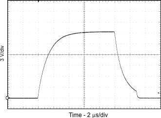
| CL = 100 nF | RG = 10 Ω | |
| VCC2 - VEE2 = VCC2 - GND2 = 20 V | ||
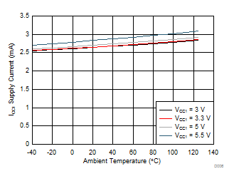
| IN+ = High | IN- = Low |
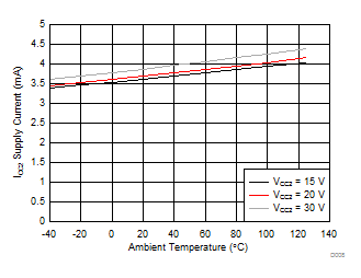
| Input Frequency = 1 kHz | ||
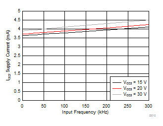
| No CL |
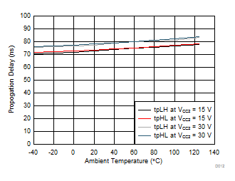
| CL = 1nF | RG = 0 Ω | VCC1 = 5 V |
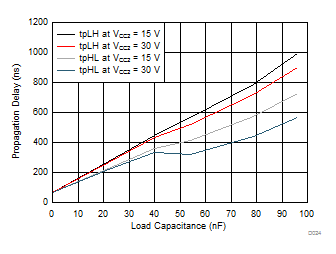
| RG = 10 Ω | VCC1 = 5 V |
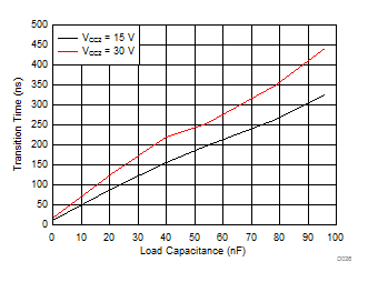
| RG = 0 Ω | VCC1 = 5 V |
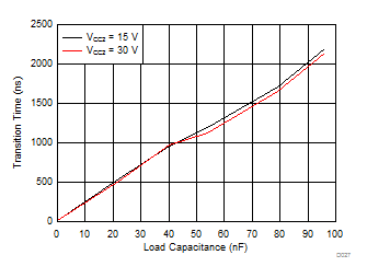
| RG = 10 Ω | VCC1 = 5 V |
| CL = 10 nF |
