ZHCSFK7A September 2016 – October 2016 TPS254900-Q1
PRODUCTION DATA.
- 1 特性
- 2 应用范围
- 3 说明
- 4 修订历史记录
- 5 Pin Configuration and Functions
- 6 Specifications
- 7 Parameter Measurement Information
-
8 Detailed Description
- 8.1 Overview
- 8.2 Functional Block Diagram
- 8.3 Feature Description
- 8.4 Device Functional Modes
- 9 Application and Implementation
- 10Power Supply Recommendations
- 11Layout
- 12器件和文档支持
- 13机械、封装和可订购信息
11 Layout
11.1 Layout Guidelines
Layout best practices for the TPS254900-Q1 are listed as follows.
- Considerations for input and output power traces
- Make the power traces as short as possible.
- Make the power traces as wide as possible.
- Considerations for input-capacitor traces
- For all applications, 10-µF and 0.1-µF low-ESR ceramic capacitors are recommended, placed close to the IN pin.
- The resistors attached to the ILIM_HI and ILIM_LO pins of the device have several requirements.
- It is recommended to use 1% low-temperature-coefficient resistors.
- The trace routing between these two pins and GND should be as short as possible to reduce parasitic effects on current limit. These traces should not have any coupling to switching signals on the board.
- Locate all TPS254900-Q1 pullup resistors for open-drain outputs close to their connection pin. Pullup resistors should be 100 kΩ.
- If a particular open-drain output is not used or needed in the system, tie it to GND.
- ESD considerations
- The TPS254900-Q1 device has built-in ESD protection for DP_IN and DM_IN. Keep trace lengths minimal from the USB connector to the DP_IN and DM_IN pins on the TPS254900-Q1 device, and use minimal vias along the traces.
- The capacitor on BIAS helps to improve the IEC ESD performance. A 2.2-µF capacitor should be placed close to BIAS, and the current path from BIAS to GND across this capacitor should be as short as possible. Do not use vias along the connection traces.
- A 10-µF output capacitor should be placed close to the OUT pin and TVS.
- See the ESD Protection Layout Guide (SLVA680) for additional information.
- TVS Considerations
- For OUT, a TVS like SMAJ18 should be placed near the OUT pin.
- For BIAS, a TVS like SMAJ18 should be placed close to the BIAS pin, but behind the 2.2-µF capacitor.
- The whole path from OUT to GND or BIAS to GND across the TVS should be as short as possible.
- DP_IN, DM_IN, DP_OUT, and DM_OUT routing considerations
- Route these traces as microstrips with nominal differential impedance of 90 Ω.
- Minimize the use of vias on the high-speed data lines.
- Keep the reference GND plane devoid from cuts or splits above the differential pairs to prevent impedance discontinuities.
- For more USB 2.0 high-speed D+ and D– differential routing information, see the High Speed USB Platform Design Guideline from Intel.
- Thermal Considerations
- When properly mounted, the thermal-pad package provides significantly greater cooling ability than an ordinary package. To operate at rated power, the thermal pad must be soldered to the board GND plane directly under the device. The thermal pad is at GND potential and can be connected using multiple vias to inner-layer GND. Other planes, such as the bottom side of the circuit board, can be used to increase heat sinking in higher-current applications. See the PowerPad™ Thermally Enhanced Package application report (SLMA002) and PowerPAD™ Made Easy application brief (SLMA004) for more information on using this thermal pad package.
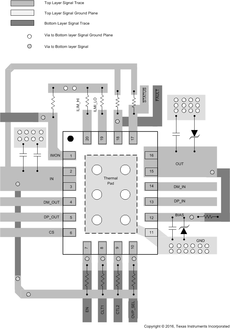
11.2 Layout Example
 Figure 54. TPS254900-Q1 Layout Diagram