ZHCSFO3D November 2016 – August 2021 LM5170-Q1
PRODUCTION DATA
- 1 特性
- 2 应用
- 3 说明
- 4 Revision History
- 5 说明(续)
- 6 Pin Configuration and Functions
- 7 Specifications
-
8 Detailed Description
- 8.1 Overview
- 8.2 Functional Block Diagram
- 8.3
Feature Description
- 8.3.1 Bias Supply (VCC, VCCA)
- 8.3.2 Undervoltage Lockout (UVLO) and Master Enable or Disable
- 8.3.3 High Voltage Input (VIN, VINX)
- 8.3.4 Current Sense Amplifier
- 8.3.5 Control Commands
- 8.3.6 Channel Current Monitor (IOUT1, IOUT2)
- 8.3.7 Cycle-by-Cycle Peak Current Limit (IPK)
- 8.3.8 Error Amplifier
- 8.3.9 Ramp Generator
- 8.3.10 Soft Start
- 8.3.11 Gate Drive Outputs, Dead Time Programming and Adaptive Dead Time (HO1, HO2, LO1, LO2, DT)
- 8.3.12 PWM Comparator
- 8.3.13 Oscillator (OSC)
- 8.3.14 Synchronization to an External Clock (SYNCIN, SYNCOUT)
- 8.3.15 Diode Emulation
- 8.3.16 Power MOSFET Failure Detection and Failure Protection (nFAULT, BRKG, BRKS)
- 8.3.17 Overvoltage Protection (OVPA, OVPB)
- 8.4 Device Functional Modes
- 8.5 Programming
-
9 Application and Implementation
- 9.1 Application Information
- 9.2
Typical Application
- 9.2.1
60-A, Dual-Phase, 48-V to 12-V Bidirectional Converter
- 9.2.1.1 Design Requirements
- 9.2.1.2
Detailed Design Procedure
- 9.2.1.2.1 Determining the Duty Cycle
- 9.2.1.2.2 Oscillator Programming
- 9.2.1.2.3 Power Inductor, RMS and Peak Currents
- 9.2.1.2.4 Current Sense (RCS)
- 9.2.1.2.5 Current Setting Limits (ISETA or ISETD)
- 9.2.1.2.6 Peak Current Limit
- 9.2.1.2.7 Power MOSFETS
- 9.2.1.2.8 Bias Supply
- 9.2.1.2.9 Boot Strap
- 9.2.1.2.10 RAMP Generators
- 9.2.1.2.11 OVP
- 9.2.1.2.12 Dead Time
- 9.2.1.2.13 IOUT Monitors
- 9.2.1.2.14 UVLO Pin Usage
- 9.2.1.2.15 VIN Pin Configuration
- 9.2.1.2.16 Loop Compensation
- 9.2.1.2.17 Soft Start
- 9.2.1.2.18 ISET Pins
- 9.2.1.3 Application Curves
- 9.2.1
60-A, Dual-Phase, 48-V to 12-V Bidirectional Converter
- 10Power Supply Recommendations
- 11Layout
- 12Device and Documentation Support
- 13Mechanical, Packaging, and Orderable Information
8.3.6 Channel Current Monitor (IOUT1, IOUT2)
The LM5170-Q1 monitors the real time inductor current in each channel at the IOUT1 and IOUT2 pins. The channel current is converted to a small current source scaled by the factors seen in Equation 11 and Equation 12:


where
- VCS1 and VCS2 are the real time current sense voltage of CH-1 and CH-2, respectively
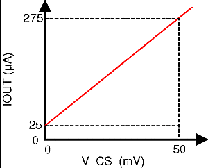
- the 25 µA is a DC offset current superimposed on to the IOUT signals (refer to Figure 8-5).
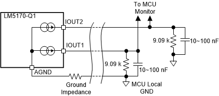
The DC offset current is introduced to raise the no-load signal above the possible ground noise floor. Because the monitor signal is in the form of current, an accurate reading can be obtained across a termination resistor even if the resistor is located far from the LM5170-Q1 but close to the MCU, thus rejecting potential ground differences between the LM5170-Q1 and the MCU. Figure 8-6 shows a typical channel current monitor through a 9.09-KΩ termination resistor and a 10-nF to 100-nF ceramic capacitor in parallel. The RC network converts the current monitor signal into a DC voltage proportional to the channel DC current. For example, when the current sense voltage DC component is 50 mVdc, namely VCS_dc = 50 mV, the termination RC network will produce a DC voltage of 2.5 V. Note that the maximum IOUT pin voltage is internally clamped to approximately 4 V.
 Figure 8-5 Channel Monitor Current Source vs Current Sense Voltage
 Figure 8-6 Channel Current Monitor