ZHCSFT4A March 2016 – August 2016 ISO7820LL , ISO7821LL
PRODUCTION DATA.
- 1 特性
- 2 应用
- 3 说明
- 4 修订历史记录
- 5 Pin Configuration and Functions
-
6 Specifications
- 6.1 Absolute Maximum Ratings
- 6.2 ESD Ratings
- 6.3 Recommended Operating Conditions
- 6.4 Thermal Information
- 6.5 Power Ratings
- 6.6 Insulation Specifications
- 6.7 Safety-Related Certifications
- 6.8 Safety Limiting Values
- 6.9 DC Electrical Characteristics
- 6.10 DC Supply Current Characteristics
- 6.11 Switching Characteristics
- 6.12 Insulation Characteristics Curves
- 6.13 Typical Characteristics
- 7 Parameter Measurement Information
- 8 Detailed Description
- 9 Application and Implementation
- 10Power Supply Recommendations
- 11Layout
- 12器件和文档支持
- 13机械、封装和可订购信息
8 Detailed Description
8.1 Overview
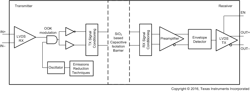
The ISO782xLL is a family of isolated LVDS buffers. The differential signal received on the LVDS input pins is first converted to CMOS logic levels. The signal is then transmitted across a silicon-dioxide (SiO2) based capacitive-isolation barrier using an on-off keying (OOK) modulation scheme. A high frequency carrier transmitted across the barrier represents one logic state and an absence of a carrier represents the other logic state. On the other side of the barrier a demodulator converts the OOK signal back to logic levels, which is then converted to LVDS outputs by a differential driver. These devices incorporate advanced circuit techniques to maximize CMTI performance and minimize radiated emissions.
The ISO782xLL family of devices is TIA/EIA-644-A standard compliant. The LVDS transmitters drive a minimum differential-output voltage magnitude of 250 mV into a 100-Ω load, and the LVDS receivers are capable of detecting differential signals ≥50 mV in magnitude. The device consumes 10 mA per channel at 100 Mbps with 5-V supplies.
The Functional Block Diagram section shows a conceptual block diagram of one channel of the ISO782xLL family of devices.
8.2 Functional Block Diagram

8.3 Feature Description
The ISO782xLL family of devices is available in two channel configurations with a default differential high-output state.
| PART NUMBER | CHANNEL DIRECTION | RATED ISOLATION | MAXIMUM DATA RATE | DEFAULT DIFFERENTIAL OUTPUT |
|---|---|---|---|---|
| ISO7820LL | 2 Forward | 5700 VRMS / 8000 VPK (1) | 100 Mbps | High |
| ISO7821LL | 1 Forward, 1 Reverse |
8.4 Device Functional Modes
Table 1 lists the functional modes for the ISO782xLL family of devices.
Table 1. ISO782xLL Function Table(1)
| VCCI | VCCO | INPUT (INx±)(2) |
OUTPUT ENABLE (ENx) |
OUTPUT (OUTx±)(3) |
COMMENTS |
|---|---|---|---|---|---|
| PU | PU | H | H or open | H | Normal Operation: A channel output assumes the logic state of the input. |
| L | H or open | L | |||
| I | H or open | H or L | |||
| X | PU | X | L | Z | A low-logic state at the output enable causes the outputs to be in high impedance. |
| PD | PU | X | H or open | H | Default mode: When VCCI is unpowered, a channel output assumes the logic high state. When VCCI transitions from unpowered to powered up, a channel output assumes the logic state of the input. When VCCI transitions from powered up to unpowered, a channel output assumes the selected default high state. |
| X | PD | X | X | Undetermined | When VCCO is unpowered, a channel output is undetermined. When VCCO transitions from unpowered to powered-up, a channel output assumes the logic state of the input |
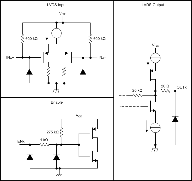
8.4.1 Device I/O Schematics
 Figure 28. Device I/O Schematics