ZHCSFV4B December 2016 – June 2017 LM5166
PRODUCTION DATA.
- 1 特性
- 2 应用
- 3 说明
- 4 修订历史记录
- 5 Pin Configuration and Functions
- 6 Specifications
-
7 Detailed Description
- 7.1 Overview
- 7.2 Functional Block Diagram
- 7.3
Feature Description
- 7.3.1 Integrated Power MOSFETs
- 7.3.2 Selectable PFM or COT Mode Converter Operation
- 7.3.3 Low Dropout Operation and 100% Duty Cycle Mode
- 7.3.4 Adjustable Output Voltage (FB)
- 7.3.5 Adjustable Current Limit
- 7.3.6 Precision Enable (EN) and Hysteresis (HYS)
- 7.3.7 Power Good (PGOOD)
- 7.3.8 Configurable Soft Start (SS)
- 7.3.9 Short-Circuit Operation
- 7.3.10 Thermal Shutdown
- 7.4 Device Functional Modes
-
8 Applications and Implementation
- 8.1 Application Information
- 8.2
Typical Applications
- 8.2.1
Design 1: Wide VIN, Low IQ, High-Efficiency COT Converter Rated at 5 V, 500 mA
- 8.2.1.1 Design Requirements
- 8.2.1.2
Detailed Design Procedure
- 8.2.1.2.1 Custom Design With WEBENCH® Tools
- 8.2.1.2.2 Feedback Resistors - RFB1, RFB2
- 8.2.1.2.3 Switching Frequency - RT
- 8.2.1.2.4 Filter Inductance - LF
- 8.2.1.2.5 Output Capacitors - COUT
- 8.2.1.2.6 Ripple Generation Network - RESR, CFF
- 8.2.1.2.7 Input Capacitor - CIN
- 8.2.1.2.8 Soft-Start Capacitor - CSS
- 8.2.1.2.9 Application Curves
- 8.2.2 Design 2: Wide VIN, Low IQ COT Converter Rated at 3.3 V, 500 mA
- 8.2.3 Design 3: High-Density PFM Converter Rated at 3.3 V, 0.3 A
- 8.2.4 Design 4: Wide VIN, Low IQ PFM Converter Rated at 5 V, 500 mA
- 8.2.5
Design 5: 12-V, 300-mA COT Converter Operating From 24-V or 48-V Input
- 8.2.5.1 Design Requirements
- 8.2.5.2
Detailed Design Procedure
- 8.2.5.2.1 Peak Current Limit Setting - RILIM
- 8.2.5.2.2 Switching Frequency - RRT
- 8.2.5.2.3 Inductor - LF
- 8.2.5.2.4 Input and Output Capacitors - CIN, COUT
- 8.2.5.2.5 Feedback Resistors - RFB1, RFB2
- 8.2.5.2.6 Ripple Generation Network - RA, CA, CB
- 8.2.5.2.7 Undervoltage Lockout Setpoint - RUV1, RUV2, RHYS
- 8.2.5.2.8 Soft Start - CSS
- 8.2.5.3 Application Curves
- 8.2.1
Design 1: Wide VIN, Low IQ, High-Efficiency COT Converter Rated at 5 V, 500 mA
- 9 Power Supply Recommendations
- 10Layout
- 11器件和文档支持
- 12机械、封装和可订购信息
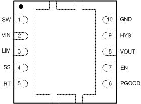
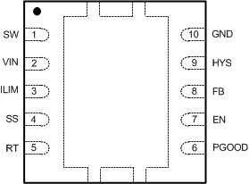
5 Pin Configuration and Functions
LM5166X and LM5166Y Fixed Output DRC Package
10-Pin VSON
Top View

LM5166 Adjustable Output DRC Package
10-Pin VSON
Top View

Pin Functions
| PIN | I/O(1) | DESCRIPTION | |
|---|---|---|---|
| NO. | NAME | ||
| 1 | SW | P | Switching node that is internally connected to the drain of the PFET buck switch (high side) and the drain of the NFET synchronous rectifier (low side). Connect to the buck inductor. |
| 2 | VIN | P | Regulator supply input pin to high-side power MOSFET and internal bias rail LDO. Connect to input supply and input filter capacitor CIN. The path from the VIN pin to the input capacitor must be as short as possible. |
| 3 | ILIM | I | Programming pin for current limit. Connecting the appropriate resistance from the ILIM pin to GND selects one of the three current limit options. The available current limit options are detailed in Table 3. |
| 4 | SS | I | Programming pin for the soft-start delay. If a 100-kΩ resistor is connected from the SS pin to GND, the internal soft-start circuit is disabled and the FB comparator reference steps immediately from zero to full value when the regulator is enabled by the EN input. If the SS pin is left open, the internal soft-start circuit ramps the FB reference from zero to full value in 900 µs. If a capacitor is connected from the SS pin to GND, the soft-start time can be set longer than 900 µs. |
| 5 | RT | I | Mode select and on-time programming pin for Constant On-Time control. Connect a resistor from the RT pin to GND to program the on-time and hence switching frequency. Short RT to GND to select PFM (pulse frequency modulation) operation. |
| 6 | PGOOD | O | Power Good output flag pin. PGOOD is connected to the drain of an NFET that holds the pin low when either FB or VOUT is not in regulation. Use a 10-kΩ to 100-kΩ pullup resistor to system voltage rail or VOUT (no higher than 12 V). |
| 7 | EN | I | Input pin of the precision enable / UVLO comparator. The regulator is enabled when the EN pin voltage is greater than 1.22 V. |
| 8 | VOUT or FB | I | Feedback input to the voltage regulation loop for the LM5166 Adjustable Output version, or a VOUT pin connects the internal feedback resistor divider to the regulator output voltage for the fixed 3.3-V or 5-V options. The FB pin connects the internal feedback comparator to an external resistor divider for the adjustable voltage option, and the reference for the FB pin comparator is 1.223 V. |
| 9 | HYS | O | Drain of internal NFET that is turned off when the EN input is greater than the EN pin threshold. External resistors from HYS to EN and GND program the input UVLO threshold and hysteresis. |
| 10 | GND | G | Regulator ground return. |
| — | PAD | P | Connect to GND pin and system ground on PCB. Path to CIN must be as short as possible. |
(1) P = Power, G = Ground, I = Input, O = Output.