ZHCSFV4B December 2016 – June 2017 LM5166
PRODUCTION DATA.
- 1 特性
- 2 应用
- 3 说明
- 4 修订历史记录
- 5 Pin Configuration and Functions
- 6 Specifications
-
7 Detailed Description
- 7.1 Overview
- 7.2 Functional Block Diagram
- 7.3
Feature Description
- 7.3.1 Integrated Power MOSFETs
- 7.3.2 Selectable PFM or COT Mode Converter Operation
- 7.3.3 Low Dropout Operation and 100% Duty Cycle Mode
- 7.3.4 Adjustable Output Voltage (FB)
- 7.3.5 Adjustable Current Limit
- 7.3.6 Precision Enable (EN) and Hysteresis (HYS)
- 7.3.7 Power Good (PGOOD)
- 7.3.8 Configurable Soft Start (SS)
- 7.3.9 Short-Circuit Operation
- 7.3.10 Thermal Shutdown
- 7.4 Device Functional Modes
-
8 Applications and Implementation
- 8.1 Application Information
- 8.2
Typical Applications
- 8.2.1
Design 1: Wide VIN, Low IQ, High-Efficiency COT Converter Rated at 5 V, 500 mA
- 8.2.1.1 Design Requirements
- 8.2.1.2
Detailed Design Procedure
- 8.2.1.2.1 Custom Design With WEBENCH® Tools
- 8.2.1.2.2 Feedback Resistors - RFB1, RFB2
- 8.2.1.2.3 Switching Frequency - RT
- 8.2.1.2.4 Filter Inductance - LF
- 8.2.1.2.5 Output Capacitors - COUT
- 8.2.1.2.6 Ripple Generation Network - RESR, CFF
- 8.2.1.2.7 Input Capacitor - CIN
- 8.2.1.2.8 Soft-Start Capacitor - CSS
- 8.2.1.2.9 Application Curves
- 8.2.2 Design 2: Wide VIN, Low IQ COT Converter Rated at 3.3 V, 500 mA
- 8.2.3 Design 3: High-Density PFM Converter Rated at 3.3 V, 0.3 A
- 8.2.4 Design 4: Wide VIN, Low IQ PFM Converter Rated at 5 V, 500 mA
- 8.2.5
Design 5: 12-V, 300-mA COT Converter Operating From 24-V or 48-V Input
- 8.2.5.1 Design Requirements
- 8.2.5.2
Detailed Design Procedure
- 8.2.5.2.1 Peak Current Limit Setting - RILIM
- 8.2.5.2.2 Switching Frequency - RRT
- 8.2.5.2.3 Inductor - LF
- 8.2.5.2.4 Input and Output Capacitors - CIN, COUT
- 8.2.5.2.5 Feedback Resistors - RFB1, RFB2
- 8.2.5.2.6 Ripple Generation Network - RA, CA, CB
- 8.2.5.2.7 Undervoltage Lockout Setpoint - RUV1, RUV2, RHYS
- 8.2.5.2.8 Soft Start - CSS
- 8.2.5.3 Application Curves
- 8.2.1
Design 1: Wide VIN, Low IQ, High-Efficiency COT Converter Rated at 5 V, 500 mA
- 9 Power Supply Recommendations
- 10Layout
- 11器件和文档支持
- 12机械、封装和可订购信息
6 Specifications
6.1 Absolute Maximum Ratings
Over the recommended operating junction temperature range of –40°C to 150°C (unless otherwise noted).(1)(2)| MIN | MAX | UNIT | ||
|---|---|---|---|---|
| VIN, EN to GND | –0.3 | 68 | V | |
| SW to GND | –0.7 | VVIN + 0.3 | V | |
| 20-ns transient | –3 | |||
| PGOOD, VOUT(3) to GND | –0.3 | 16 | V | |
| HYS to GND | –0.3 | 7 | V | |
| ILIM, SS, RT, FB(4) to GND | –0.3 | 3.6 | V | |
| Maximum junction temperature, TJ | –40 | 150 | °C | |
| Storage temperature, Tstg | –55 | 150 | °C | |
(1) Stresses beyond those listed under Absolute Maximum Ratings may cause permanent damage to the device. These are stress ratings only, which do not imply functional operation of the device at these or any other conditions beyond those indicated under Recommended Operating Conditions. Exposure to absolute-maximum-rated conditions for extended periods may affect device reliability.
(2) If Military/Aerospace specified devices are required, please contact the Texas Instruments Sales Office/Distributors for availability and specifications.
(3) Fixed output setting.
(4) Adjustable output setting.
6.2 ESD Ratings
| VALUE | UNIT | |||
|---|---|---|---|---|
| V(ESD) | Electrostatic discharge | Human body model (HBM), per ANSI/ESDA/JEDEC JS-001(1) | ±2000 | V |
| Charged device model (CDM), per JEDEC specification JESD22-C101(2) | ±1000 | |||
(1) JEDEC document JEP155 states that 500-V HBM allows safe manufacturing with a standard ESD control process.
(2) JEDEC document JEP157 states that 250-V CDM allows safe manufacturing with a standard ESD control process.
6.3 Recommended Operating Conditions
Over the recommended operating junction temperature range of –40°C to 150°C (unless otherwise noted).(1)| MIN | NOM | MAX | UNIT | ||
|---|---|---|---|---|---|
| Input voltages | VIN | 3 | 65 | V | |
| EN | –0.3 | 65 | |||
| PGOOD | –0.3 | 12 | |||
| HYS | –0.3 | 5.5 | |||
| Output current | IOUT | 0 | 500 | mA | |
| Temperature | Operating junction temperature | –40 | 150 | °C | |
(1) Operating Ratings are conditions under which the device is intended to be functional. For specifications and test conditions, see Electrical Characteristics.
6.4 Thermal Information
| THERMAL METRIC(1) | LM5166 | UNIT | |
|---|---|---|---|
| DRC (VSON) | |||
| 10 PINS | |||
| RθJA | Junction-to-ambient thermal resistance | 49.1 | °C/W |
| RθJC(top) | Junction-to-case (top) thermal resistance | 57.2 | °C/W |
| RθJB | Junction-to-board thermal resistance | 26.6 | °C/W |
| ψJT | Junction-to-top characterization parameter | 0.8 | °C/W |
| ψJB | Junction-to-board characterization parameter | 23.8 | °C/W |
| RθJC(bot) | Junction-to-case (bottom) thermal resistance | 4.8 | °C/W |
(1) For more information about traditional and new thermal metrics, see the Semiconductor and IC Package Thermal Metrics application report.
6.5 Electrical Characteristics
Typical values correspond to TJ = 25°C. Minimum and maximum limits are based on TJ = –40°C to +125°C. VIN = 12 V (unless otherwise noted).(1)(2)| PARAMETER | TEST CONDITIONS | MIN | TYP | MAX | UNIT | |
|---|---|---|---|---|---|---|
| IQ-SD | VIN DC supply current, shutdown | VEN = 0 V, TJ = 25°C | 4 | 6 | µA | |
| IQ-SLEEP | VIN DC supply current, no load | VFB = 1.5 V, TJ = 25°C | 9.7 | 15 | µA | |
| IQ-SLEEP-VINMAX | VIN DC supply current, no load | VFB = 1.5 V, VVIN = 65 V, TJ = 25°C | 10 | 15 | µA | |
| IQ-ACTIVE-PFM | VIN DC supply current, active | PFM mode, RRT = 0 Ω, RSS = 100 kΩ | 205 | µA | ||
| IQ-ACTIVE-COT | VIN DC supply current, active | COT mode, RRT = RSS = 100 kΩ | 320 | µA | ||
| POWER SWITCHES | ||||||
| RDSON1 | High-side MOSFET RDS(on) | ISW = –100 mA | 0.93 | Ω | ||
| RDSON2 | Low-side MOSFET RDS(on) | ISW = 100 mA | 0.48 | Ω | ||
| CURRENT LIMITING | ||||||
| IHS_LIM1 | High-side peak current limit threshold | See Table 3 | 1125 | 1250 | 1375 | mA |
| IHS_LIM2 | 675 | 750 | 825 | |||
| IHS_LIM3 | 440 | 500 | 560 | |||
| ILS_LIM1 | Low-side valley current limit threshold | See Table 3 | 415 | mA | ||
| ILS_LIM2 | 315 | |||||
| REGULATION COMPARATOR | ||||||
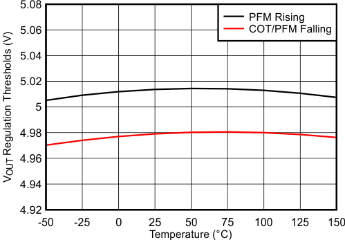
| VVOUT5 | VOUT 5-V DC setpoint | LM5166X | 4.9 | 5.0 | 5.1 | V |
| VVOUT3.3 | VOUT 3.3-V DC setpoint | LM5166Y | 3.23 | 3.3 | 3.37 | V |
| IVOUT | VOUT pin input current | VVOUT = 5 V, LM5166X | 7 | µA | ||
| VVOUT = 3.3 V, LM5166Y | 3.8 | |||||
| VFB1 | Lower FB regulation threshold (PFM and COT) |
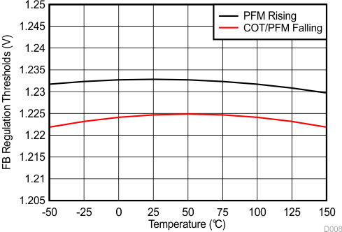
Adjustable VOUT version | 1.208 | 1.223 | 1.238 | V |
| VFB2 | Upper FB regulation threshold (PFM) | 1.218 | 1.233 | 1.248 | V | |
| IFB | FB pin input bias current | VFB = 1 V | 25 | nA | ||
| FBHYS-PFM | FB comparator PFM hysteresis | PFM mode | 10 | mV | ||
| FBHYS-COT | FB comparator dropout hysteresis | COT mode | 4 | mV | ||
| FBLINE-REG | FB threshold variation over line | VVIN = 3 V to 65 V | 0.005 | %/V | ||
| VOUTLINE-REG | VOUT threshold variation over line | LM5166X, VVIN = 6 V to 65 V LM5166Y, VVIN = 4.5 V to 65 V |
0.005 | %/V | ||
| POWER GOOD | ||||||
| UVTRISING | PGOOD comparator | VFB rising relative to VFB1 threshold | 94% | |||
| UVTFALLING | VFB falling relative to VFB1 threshold | 87% | ||||
| RPGOOD | PGOOD on-resistance | VFB = 1 V | 80 | 200 | Ω | |
| VINMIN-PGOOD | Minimum required VIN for valid PGOOD | VVIN falling IPGOOD = 0.1 mA, VPGOOD < 0.5 V |
1.2 | 1.65 | V | |
| IPGOOD | PGOOD off-state leakage | VFB = 1.2 V, VPGOOD = 5.5 V | 10 | 100 | nA | |
| ENABLE / UVLO | ||||||
| VIN-ON | Turnon threshold | VVIN rising | 2.60 | 2.75 | 2.95 | V |
| VIN-OFF | Turnoff threshold | VVIN falling | 2.35 | 2.45 | 2.60 | V |
| VEN-ON | EN turnon threshold | VEN rising | 1.163 | 1.22 | 1.276 | V |
| VEN-OFF | EN turnoff threshold | VEN falling | 1.109 | 1.144 | 1.178 | V |
| VEN-HYS | EN hysteresis | 76 | mV | |||
| VEN-SD | EN shutdown threshold | VEN falling | 0.3 | 0.6 | V | |
| RHYS | HYS on-resistance | VEN = 1 V | 80 | 200 | Ω | |
| IHYS | HYS off-state leakage | VEN = 1.5 V, VHYS = 5.5 V | 10 | 100 | nA | |
| SOFT-START | ||||||
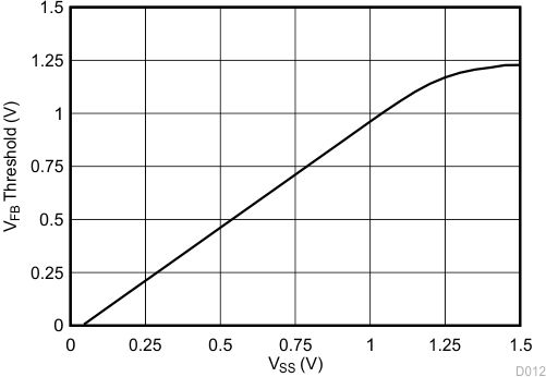
| ISS | Soft-start charging current | VSS = 1 V | 10 | µA | ||
| TSS-INT | Soft-start rise time | SS floating | 900 | µs | ||
| THERMAL SHUTDOWN | ||||||
| TJ-SD | Thermal shutdown threshold | 170 | °C | |||
| TJ-SD-HYS | Thermal shutdown hysteresis | 10 | °C | |||
6.6 Switching Characteristics
Over operating free-air temperature range (unless otherwise noted)| PARAMETER | TEST CONDITIONS | MIN | TYP | MAX | UNIT | |
|---|---|---|---|---|---|---|
| TON-MIN | Minimum on-time | 180 | ns | |||
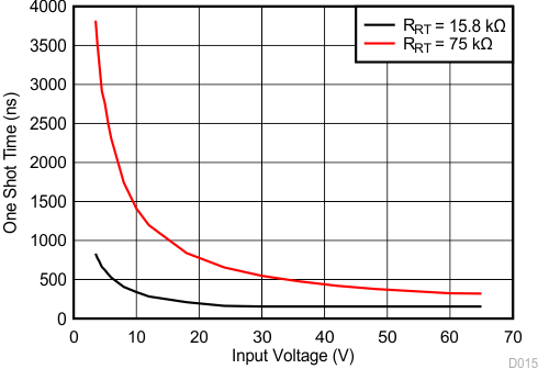
| TON1 | On-time | 16 kΩ from RT to GND | 280 | ns | ||
| TON2 | On-time | 75 kΩ from RT to GND | 1150 | ns | ||
(1) All hot and cold limits are specified by correlating the electrical characteristics to process and temperature variations and applying statistical process control.
(2) The junction temperature (TJ in °C) is calculated from the ambient temperature (TA in °C) and power dissipation (PD in Watts) as follows: TJ = TA + (PD • θJA) where θJA (in °C/W) is the package thermal impedance provided in Thermal Information.
6.7 Typical Characteristics
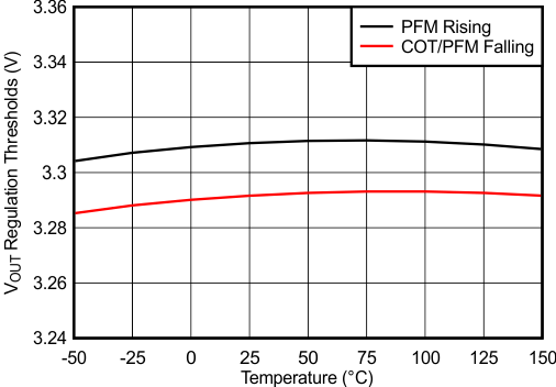
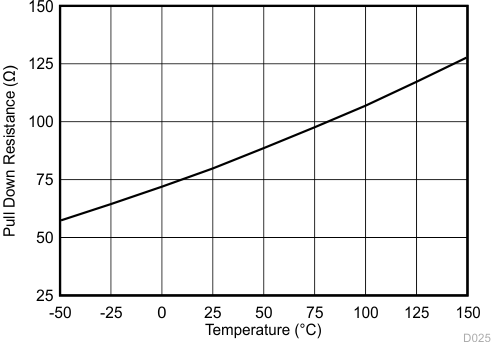
Unless otherwise specified, VIN = 12 V, VOUT = 5 V. Please refer to Typical Applications for circuit designs.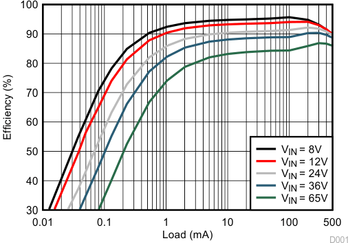
| See schematic, Figure 52 |
LF = 150 µH COUT = 47 µF |
FSW(nom) = 100 kHz RRT = 309 kΩ |
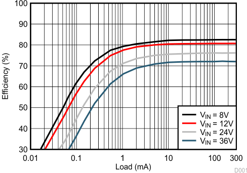
| See schematic, Figure 70 |
LF = 4.7 µH COUT = 47 µF |
FSW(nom) = 600 kHz RRT = 0 Ω |
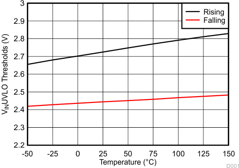
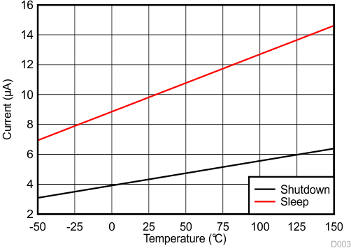
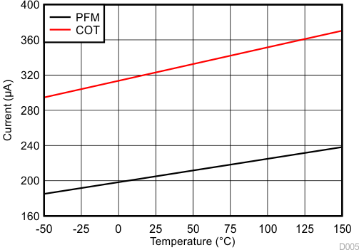
| RRT = 100 kΩ |
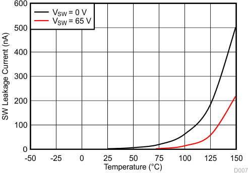
| VVIN = 65 V |
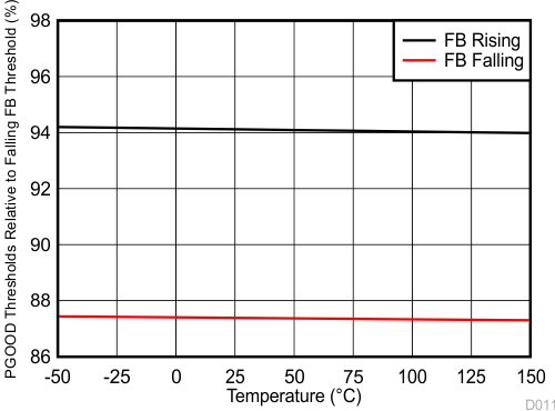
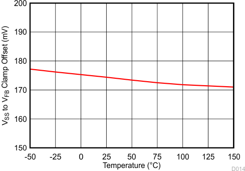
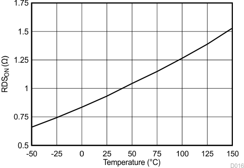
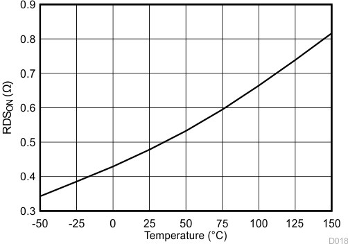
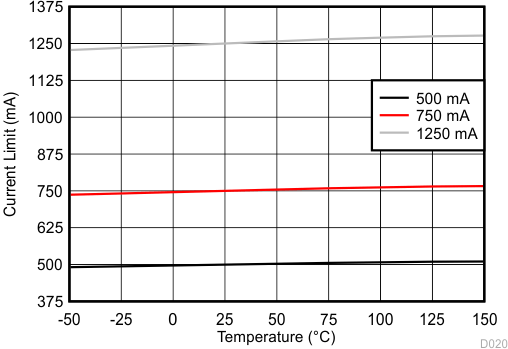
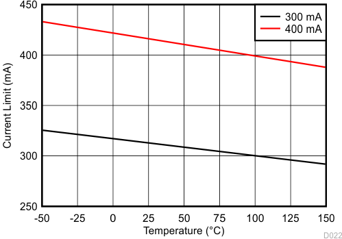
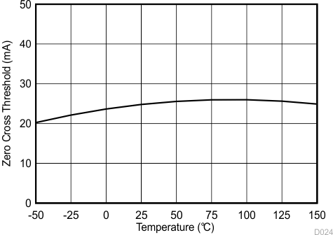
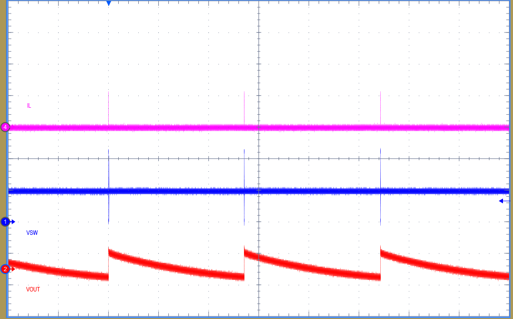
| Time Scale: 20 ms/Div CH1: VSW, 5 V/Div |
CH2: VOUT, 50 mV/Div CH4: IL, 200 mA/Div |
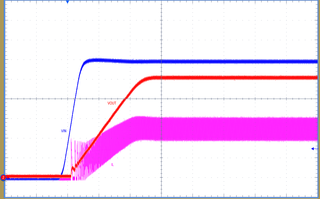
| Time Scale: 2 ms/Div CH1: VIN, 2 V/Div |
CH2: VOUT, 1 V/Div CH4: IL, 200 mA/Div |
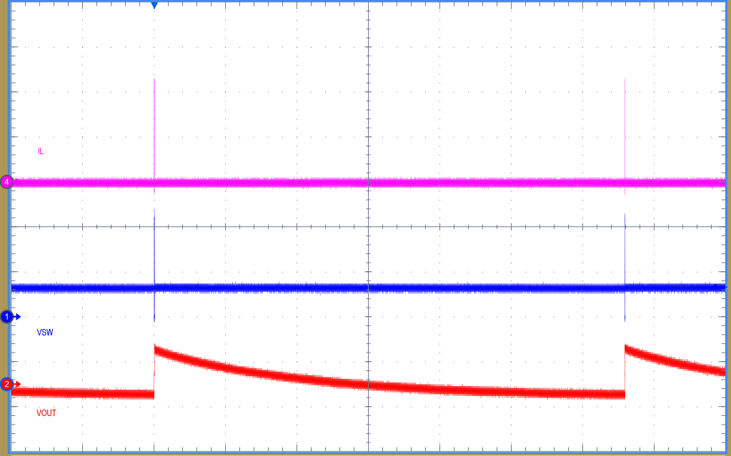
| Time Scale: 20 ms/Div CH1: VSW, 5 V/Div |
CH2: VOUT, 50 mV/Div CH4: IL, 400 mA/Div |
PFM Mode, ILIM = 750 mA
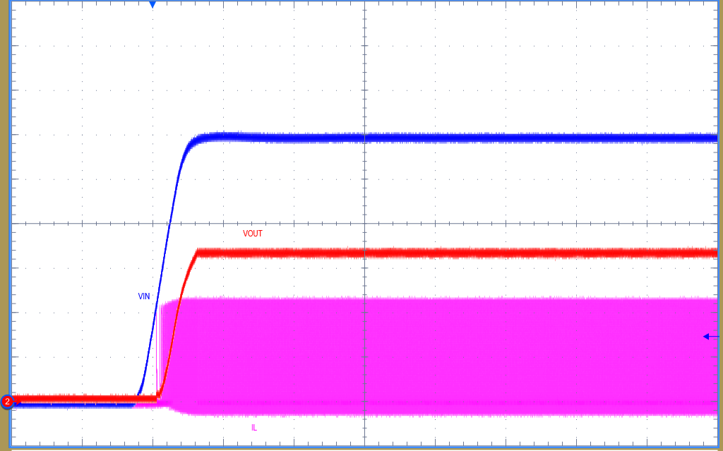
| Time Scale: 2 ms/Div CH1: VIN, 2 V/Div |
CH2: VOUT, 1 V/Div CH4: IL, 400 mA/Div |
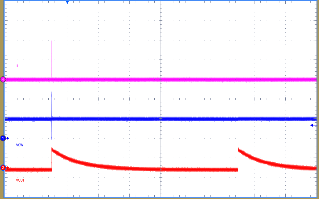
| Time Scale: 50 ms/Div CH1: VSW, 5 V/Div |
CH2: VOUT, 50 mV/Div CH4: IL, 400 mA/Div |
PFM Mode, ILIM = 1.25 A, Modulated
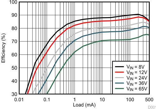
| See schematic, Figure 63 |
LF = 47 µH COUT = 47 µF |
FSW(nom) = 200 kHz RRT = 100 kΩ |
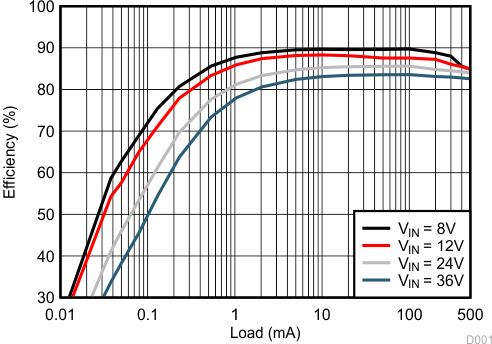
| See schematic, Figure 77 |
LF = 22 µH COUT = 200 µF |
FSW(nom) = 100 kHz RRT = 0 Ω |
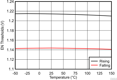
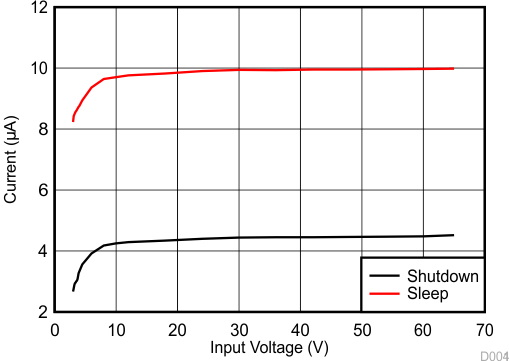
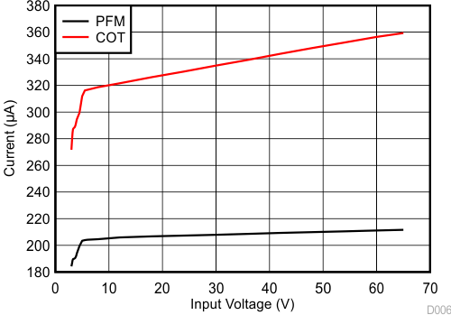
| RRT = 100 kΩ |
| LM5166X |
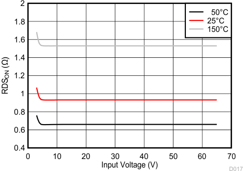
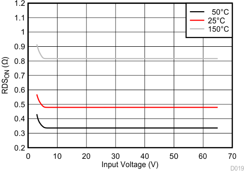
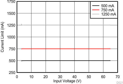
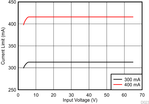
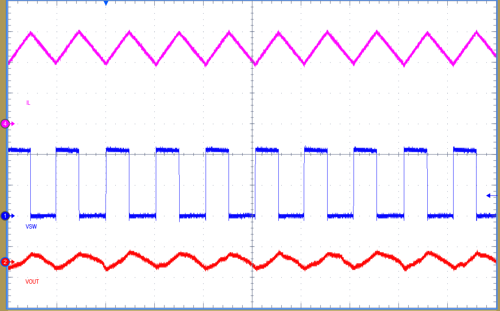
| Time Scale: 10 µs/Div CH1: VSW, 5 V/Div |
CH2: VOUT, 50 mV/Div CH4: IL, 200 mA/Div |
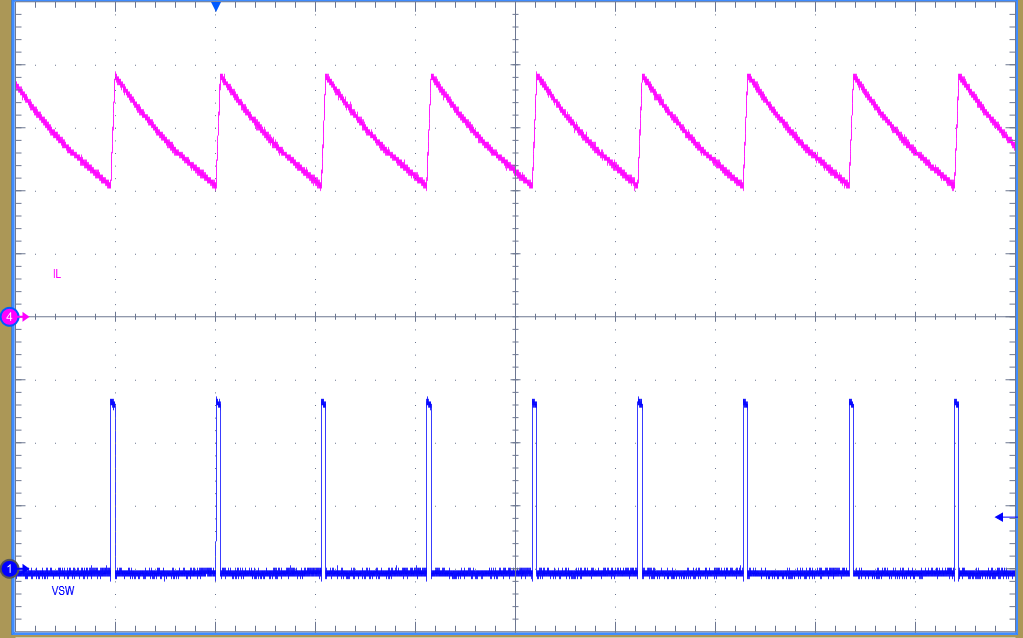
| Time Scale: 100 µs/Div CH1: VSW, 4 V/Div |
CH4: IL, 200 mA/Div |
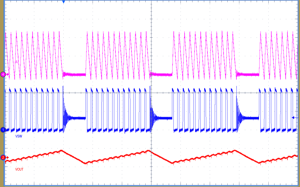
| Time Scale: 10 µs/Div CH1: VSW, 5 V/Div |
CH2: VOUT, 100 mV/Div CH4: IL, 400 mA/Div |
PFM Mode, ILIM = 750 mA
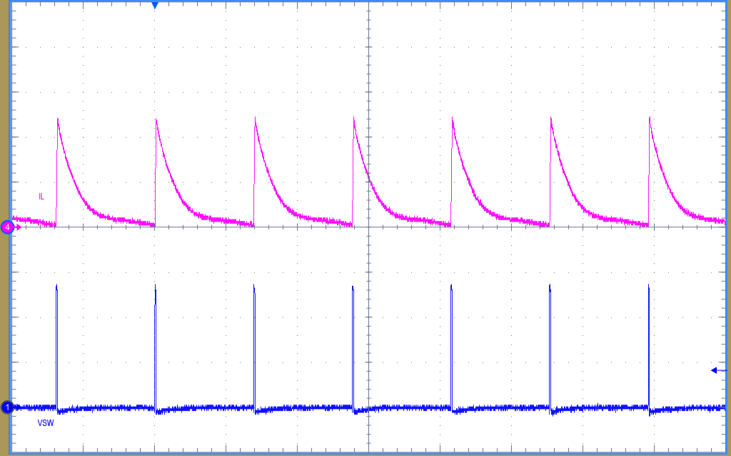
| Time Scale: 20 µs/Div CH1: VSW, 4 V/Div |
CH4: IL, 400 mA/Div |
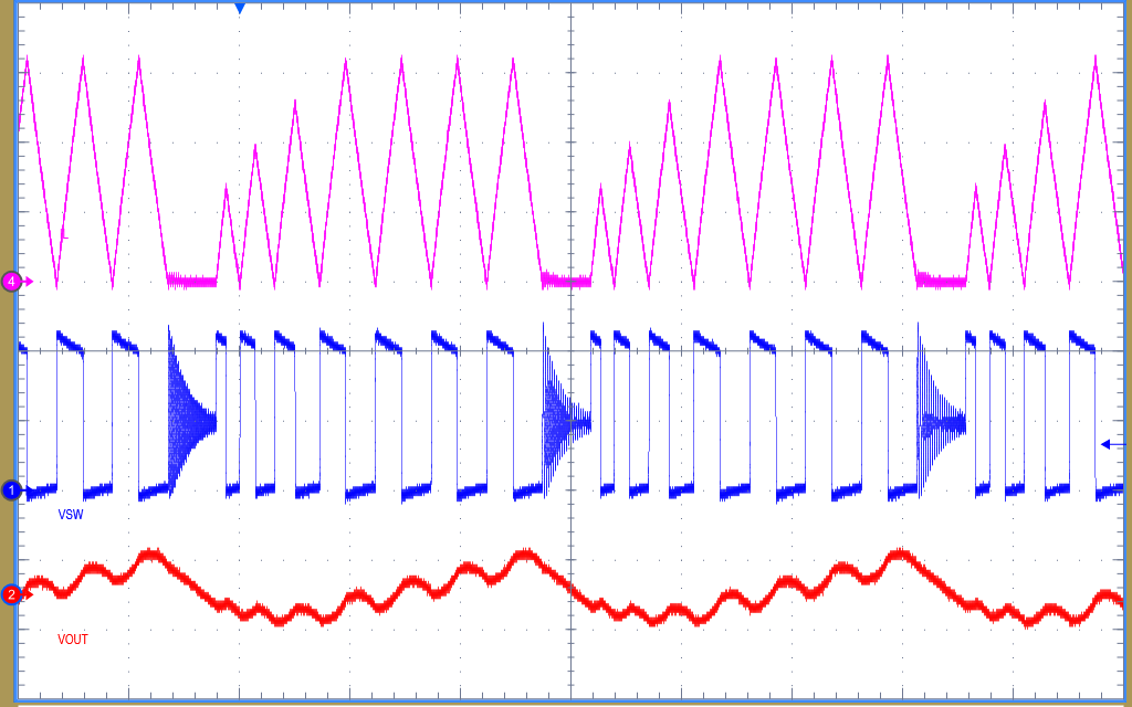
| Time Scale: 20 µs/Div CH1: VSW, 5 V/Div |
CH2: VOUT, 100 mV/Div CH4: IL, 400 mA/Div |
PFM Mode, ILIM = 1.25 A, Modulated
