ZHCSFV6E august 2016 – november 2020 DS90UB933-Q1
PRODUCTION DATA
- 1
- 1 特性
- 2 应用
- 3 说明
- 4 Revision History
- 5 Pin Configuration and Functions
-
6 Specifications
- 6.1 Absolute Maximum Ratings
- 6.2 ESD Ratings
- 6.3 Recommended Operating Conditions
- 6.4 Thermal Information
- 6.5 Electrical Characteristics
- 6.6 Recommended Serializer Timing For PCLK
- 6.7 AC Timing Specifications (SCL, SDA) - I2C-Compatible
- 6.8 Bidirectional Control Bus DC Timing Specifications (SCL, SDA) - I2C-Compatible
- 6.9 Serializer Switching Characteristics
- 6.10 Timing Diagrams
- 6.11 Typical Characteristics
- 7 Detailed Description
- 8 Application and Implementation
- 9 Power Supply Recommendations
- 10Layout
- 11Device and Documentation Support
10.2 Layout Example
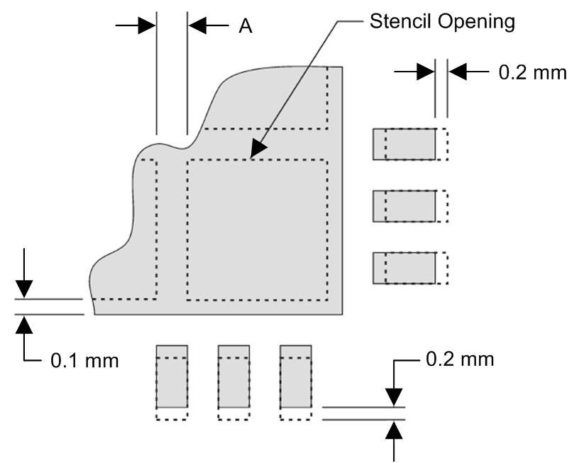
Stencil parameters such as aperture area ratio and the fabrication process have a significant impact on paste deposition. Inspection of the stencil prior to placement of the WQFN package is highly recommended to improve board assembly yields. If the via and aperture openings are not carefully monitored, the solder may flow unevenly through the DAP. Stencil parameters for aperture opening and via locations are shown in the following:
 Figure 10-1 No Pullback WQFN, Single Row Reference Diagram
| DEVICE | PIN COUNT | MKT DWG | PCB I/O PAD SIZE (mm) | PCB PITCH (mm) | PCB DAP SIZE(mm) | STENCIL I/O APERTURE (mm) | STENCIL DAP APERTURE (mm) | NUMBER OF DAP APERTURE OPENINGS | GAP BETWEEN DAP APERTURE (Dim A mm) |
|---|---|---|---|---|---|---|---|---|---|
| DS90UB933-Q1 | 32 | RTV | 0.25 × 0.6 | 0.5 | 3.1 × 3.1 | 0.25 × 0.7 | 1.4 × 1.4 | 4 | 0.2 |
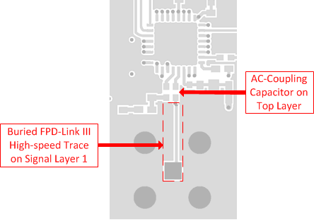
 Figure 10-2 DS90UB933-Q1 Serializer DOUT+ Trace Layout
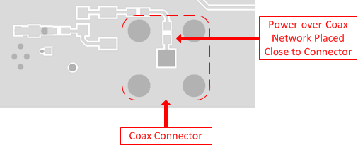
 Figure 10-3 DS90UB933-Q1 Power-over-Coax Layout
Figure 10-2 and Figure 10-3 are derived from the layout design of the DS90UB933-Q1 evaluation module (EVM). The EVM is designed for coax operation. The trace carrying high-speed serial signal DOUT+ is critical and must be kept as short as possible. Burying this trace in an internal PCB layer may help reduce emissions. If Power-over-Coax is used, the stub must be minimized by placing the filter network as close as possible to the coax connector. These graphics and additional layout description are used to demonstrate both proper routing and proper solder techniques when designing in this serializer.