ZHCSFV6E august   2016  – november 2020 DS90UB933-Q1

PRODUCTION DATA  

  1.   1
  2. 特性
  3. 应用
  4. 说明
  5. Revision History
  6. Pin Configuration and Functions
    1.     Pin Functions
  7. Specifications
    1. 6.1  Absolute Maximum Ratings
    2. 6.2  ESD Ratings
    3. 6.3  Recommended Operating Conditions
    4. 6.4  Thermal Information
    5. 6.5  Electrical Characteristics
    6. 6.6  Recommended Serializer Timing For PCLK
    7. 6.7  AC Timing Specifications (SCL, SDA) - I2C-Compatible
    8. 6.8  Bidirectional Control Bus DC Timing Specifications (SCL, SDA) - I2C-Compatible
    9. 6.9  Serializer Switching Characteristics
    10. 6.10 Timing Diagrams
    11. 6.11 Typical Characteristics
  8. Detailed Description
    1. 7.1 Overview
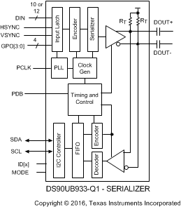
    2. 7.2 Functional Block Diagram
    3. 7.3 Feature Description
      1. 7.3.1 Serial Frame Format
      2. 7.3.2 Line Rate Calculations for the DS90UB933/934
      3. 7.3.3 Error Detection
      4. 7.3.4 Synchronizing Multiple Cameras
      5. 7.3.5 General Purpose I/O (GPIO) Descriptions
      6. 7.3.6 LVCMOS V(VDDIO) Option
      7. 7.3.7 Pixel Clock Edge Select (TRFB / RRFB)
      8. 7.3.8 Power Down
    4. 7.4 Device Functional Modes
      1. 7.4.1 DS90UB933/934 Operation With External Oscillator as Reference Clock
      2. 7.4.2 DS90UB933/934 Operation With Pixel Clock From Imager as Reference Clock
      3. 7.4.3 MODE Pin on Serializer
      4. 7.4.4 Internal Oscillator
      5. 7.4.5 Built-In Self Test
      6. 7.4.6 BIST Configuration and Status
      7. 7.4.7 Sample BIST Sequence
    5. 7.5 Programming
      1. 7.5.1 Programmable Controller
      2. 7.5.2 Description of Bidirectional Control Bus and I2C Modes
      3. 7.5.3 I2C Pass-Through
      4. 7.5.4 Slave Clock Stretching
      5. 7.5.5 IDX Address Decoder on the Serializer
      6. 7.5.6 Multiple Device Addressing
    6. 7.6 Register Maps
  9. Application and Implementation
    1. 8.1 Application Information
      1. 8.1.1 Power Over Coax
      2. 8.1.2 Power-Up Requirements and PDB Pin
      3. 8.1.3 AC Coupling
      4. 8.1.4 Transmission Media
    2. 8.2 Typical Applications
      1. 8.2.1 Coax Application
        1. 8.2.1.1 Design Requirements
        2. 8.2.1.2 Detailed Design Procedure
        3. 8.2.1.3 Application Curves
      2. 8.2.2 STP Application
        1. 8.2.2.1 Design Requirements
        2. 8.2.2.2 Detailed Design Procedure
        3. 8.2.2.3 62
  10. Power Supply Recommendations
  11. 10Layout
    1. 10.1 Layout Guidelines
      1. 10.1.1 Interconnect Guidelines
    2. 10.2 Layout Example
  12. 11Device and Documentation Support
    1. 11.1 Documentation Support
      1. 11.1.1 Related Documentation
    2. 11.2 Receiving Notification of Documentation Updates
    3. 11.3 支持资源
    4. 11.4 Trademarks
    5. 11.5 静电放电警告
    6. 11.6 术语表

Functional Block Diagram

GUID-846D53F2-C939-4B64-9700-0EF77DCB95AC-low.gif