ZHCSFV6E august 2016 – november 2020 DS90UB933-Q1
PRODUCTION DATA
- 1
- 1 特性
- 2 应用
- 3 说明
- 4 Revision History
- 5 Pin Configuration and Functions
-
6 Specifications
- 6.1 Absolute Maximum Ratings
- 6.2 ESD Ratings
- 6.3 Recommended Operating Conditions
- 6.4 Thermal Information
- 6.5 Electrical Characteristics
- 6.6 Recommended Serializer Timing For PCLK
- 6.7 AC Timing Specifications (SCL, SDA) - I2C-Compatible
- 6.8 Bidirectional Control Bus DC Timing Specifications (SCL, SDA) - I2C-Compatible
- 6.9 Serializer Switching Characteristics
- 6.10 Timing Diagrams
- 6.11 Typical Characteristics
- 7 Detailed Description
- 8 Application and Implementation
- 9 Power Supply Recommendations
- 10Layout
- 11Device and Documentation Support
8.1.2 Power-Up Requirements and PDB Pin
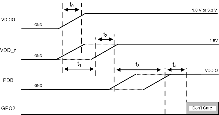
Transition of the PDB pin from LOW to HIGH must occur after the VVDDIO and VVDD_n supplies have reached their required operating voltage levels. Direct control of the PDB timing by processor GPIO is recommended if possible. When direct control of PDB is not available, the PDB pin can be tied to the power supply rail with an RC filter network to help ensure proper power up timing. GPO2 should be low when PDB goes high. Timing constraints are noted in Suggested Power-Up Sequencing and Power-Up Sequencing Constraints. Please refer to Power Down section for device operation when powered down.
If GPO2 state is not determined when PDB goes high, DS90UB933-Q1 registers must be programmed to configure the transmission mode. Mode Select register 0x05[5] must be set to 1 and register 0x05 bit 1 and 0 are to be selected based on desired 12-bit or 10-bit transmit data format.
Common applications tie the V(VDDIO) and V(VDD_n) supplies to the same power source of 1.8 V typically. This is an acceptable method for ramping the V(VDDIO) and V(VDD_n) supplies. The main constraint here is that the V(VDD_n) supply does not lead in ramping before the V(VDDIO) system supply. This is noted in Suggested Power-Up Sequencing with the requirement of t1 ≥ 0. V(VDDIO) must reach the expected operating voltage earlier than V(VDD_n) or at the same time.
 Figure 8-1 Suggested Power-Up Sequencing
| SYMBOL | DESCRIPTION | TEST CONDITIONS | MIN | TYP | MAX | Units |
|---|---|---|---|---|---|---|
| t0 | V(VDDIO) rise time | 10% to 90% of nominal voltage on rising edge. Monotonic signal ramp is required | 0.05 | 5 | ms | |
| t1 | V(VDDIO) to V(VDD_n) delay | 10% of rising edge (V(VDDIO)) to 10% of rising edge (V(VDD_n)) | 0 | ms | ||
| t2 | V(VDD_n) rise time | 10% to 90% of nominal voltage on rising edge. Monotonic signal ramp is required. VPDB < 10% of V(VDDIO) | 0.05 | 5 | ms | |
| t3* | V(VDD_n) to PDB VIH delay | 90% rising edge (V(VDD_n)) to PDB VIH | 0 | 16 | ms | |
| t4 | PDB to GPO2 delay | PDB VIH to 10% of rising edge (GPO2) | 1.3 | ms |
* If timing constraint t3 cannot be assured, the following programming steps should be issued to the via local I2C control (not via remote back channel). These programming steps should be completed > 10ms after the power sequence is complete (VPDB > PDB VIH) with no delay between write commands. This step will cause a brief restart of the forward channel output:
- Write Register 0x27 = 0x28
- Write Register 0x27 = 0x20
- Write Register 0x27 = 0x00