ZHCSFZ0D December 2016 – December 2023 DAC38RF80 , DAC38RF83 , DAC38RF84 , DAC38RF85 , DAC38RF90 , DAC38RF93
PRODUCTION DATA
- 1
- 1 特性
- 2 应用
- 3 说明
- 4 Device Comparison
- 5 Pin Configuration and Functions
-
6 Specifications
- 6.1 Absolute Maximum Ratings
- 6.2 ESD Ratings
- 6.3 Recommended Operating Conditions
- 6.4 Thermal Information
- 6.5 Electrical Characteristics - DC Specifications
- 6.6 Electrical Characteristics - Digital Specifications
- 6.7 Electrical Characteristics - AC Specifications
- 6.8 PLL/VCO Electrical Characteristics
- 6.9 Timing Requirements
- 6.10 Typical Characteristics
-
7 Detailed Description
- 7.1 Overview
- 7.2 Functional Block Diagrams
- 7.3
Feature Description
- 7.3.1 SerDes Inputs
- 7.3.2 SerDes Rate
- 7.3.3 SerDes PLL
- 7.3.4 SerDes Equalizer
- 7.3.5 JESD204B Descrambler
- 7.3.6 JESD204B Frame Assembly
- 7.3.7 SYNC Interface
- 7.3.8 Single or Dual Link Configuration
- 7.3.9 Multi-Device Synchronization
- 7.3.10 SYSREF Capture Circuit
- 7.3.11 SerDes Test Modes through Serial Programming
- 7.3.12 SerDes Test Modes through IEEE 1500 Programming
- 7.3.13 Error Counter
- 7.3.14 Eye Scan
- 7.3.15 JESD204B Pattern Test
- 7.3.16 Multiband DUC (multi-DUC)
- 7.3.17 PA Protection Block
- 7.3.18 Gain Block
- 7.3.19 Output Summation
- 7.3.20 Output Delay
- 7.3.21 Polarity Inversion
- 7.3.22 Temperature Sensor
- 7.3.23 Alarm Monitoring
- 7.3.24 Differential Clock Inputs
- 7.3.25 CMOS Digital Inputs
- 7.3.26 DAC Fullscale Output Current
- 7.3.27 Current Steering DAC Architecture
- 7.3.28 DAC Transfer Function for DAC38RF83, 93, 85
- 7.3.29 DAC Transfer Function for DAC38RF80/90/84
- 7.4 Device Functional Modes
- 7.5
Register Maps
- 7.5.1 Chip Reset and Configuration Register (address = 0x00) [reset = 0x5803]
- 7.5.2 IO Configuration Register (address = 0x01) [reset = 0x1800]
- 7.5.3 Lane Single Detect Alarm Mask Register (address = 0x02) [reset = 0xFFFF]
- 7.5.4 Clock Alarms Mask Register (address = 0x03) [reset = 0xFFFF
- 7.5.5 SERDES Loss of Signal Detection Alarms Register (address = 0x04) [reset = 0x0000]
- 7.5.6 SYSREF Alignment Circuit Alarms Register (address = 0x05) [reset = variable]
- 7.5.7 Temperature Sensor and PLL Loop Voltage Register (address = 0x06) [reset = variable]
- 7.5.8 Page Set Register (address = 0x09) [reset = 0x0000]
- 7.5.9 SYSREF Align to r1 and r3 Count Register (address = 0x78) [reset = 0x0000]
- 7.5.10 SYSREF Phase Count 1 and 2 Register (address = 0x79) [reset = 0x0000]
- 7.5.11 SYSREF Phase Count 3 and 4 Register (address = 0x7A) [reset = 0x0000]
- 7.5.12 Vendor ID and Chip Version Register (address = 0x7F) [reset = 0x0009]
- 7.5.13 Multi-DUC Configuration (PAP, Interpolation) Register (address = 0x0A) [reset = 0x02B0]
- 7.5.14 Multi-DUC Configuration (Mixers) Register (address = 0x0C) [reset = 0x2402]
- 7.5.15 JESD FIFO Control Register (address = 0x0D)[reset = 0x8000]
- 7.5.16 Alarm Mask 1 Register (address = 0x0E) [reset = 0x00FF]
- 7.5.17 Alarm Mask 2 Register (address = 0x0F) [reset = 0xFFFF]
- 7.5.18 Alarm Mask 3 Register (address = 0x10) [reset = 0xFFFF]
- 7.5.19 Alarm Mask 4 Register (address = 0x11) [reset = 0xFFFF]
- 7.5.20 JESD Lane Skew Register (address = 0x12) [reset = 0x0000]
- 7.5.21 CMIX Configuration Register (address = 0x17) [reset = 0x0000]
- 7.5.22 Output Summation and Delay Register (address = 0x19) [reset = 0x0000]
- 7.5.23 NCO Phase Path AB Register (address = 0x1C) [reset = 0x0000]
- 7.5.24 NCO Phase Path CD Register (address = 0x1D) [reset = 0x0000]
- 7.5.25 NCO Frequency Path AB Register (address = 0x1E-0x20) [reset = 0x0000 0000 0000]
- 7.5.26 NCO Frequency Path CD Register (address = 0x21-0x23) [reset = 0x0000 0000 0000]
- 7.5.27 SYSREF Use for Clock Divider Register (address = 0x24) [reset = 0x0010]
- 7.5.28 Serdes Clock Control Register (address = 0x25) [reset = 0x7700]
- 7.5.29 Sync Source Control 1 Register (address = 0x27) [reset = 0x1144]
- 7.5.30 Sync Source Control 2 Register (address = 0x28) [reset = 0x0000]
- 7.5.31 PAP path AB Gain Attenuation Step Register (address = 0x29) [reset = 0x0000]
- 7.5.32 PAP path AB Wait Time Register (address = 0x2A) [reset = 0x0000]
- 7.5.33 PAP path CD Gain Attenuation Step Register (address = 0x2B) [reset = 0x0000]
- 7.5.34 PAP Path CD Wait Time Register (address = 0x2C) [reset = 0x0000]
- 7.5.35 PAP path AB Configuration Register (address = 0x2D) [reset = 0x0FFF]
- 7.5.36 PAP path CD Configuration Register (address = 0x2E) [reset = 0x0FFF]
- 7.5.37 DAC SPI Configuration Register (address = 0x2F) [reset = 0x0000]
- 7.5.38 DAC SPI Constant Register (address = 0x30) [reset = 0x0000]
- 7.5.39 Gain for path AB Register (address = 0x32) [reset = 0x0400]
- 7.5.40 Gain for path CD Register (address = 0x33) [reset = 0x0400]
- 7.5.41 JESD Error Counter Register (address = 0x41) [reset = 0x0000]
- 7.5.42 JESD ID 1 Register (address = 0x46) [reset = 0x0044]
- 7.5.43 JESD ID 2 Register (address = 0x47) [reset = 0x190A]
- 7.5.44 JESD ID 3 and Subclass Register (address = 0x48) [reset = 0x31C3]
- 7.5.45 JESD Lane Enable Register (address = 0x4A) [reset = 0x0003]
- 7.5.46 JESD RBD Buffer and Frame Octets Register (address = 0x4B) [reset = 0x1300]
- 7.5.47 JESD K and L Parameters Register (address = 0x4C) [reset = 0x1303]
- 7.5.48 JESD M and S Parameters Register (address = 0x4D) [reset = 0x0100]
- 7.5.49 JESD N, HD and SCR Parameters Register (address = 0x4E) [reset = 0x0F4F]
- 7.5.50 JESD Character Match and Other Register (address = 0x4F) [reset = 0x1CC1]
- 7.5.51 JESD Link Configuration Data Register (address = 0x50) [reset = 0x0000]
- 7.5.52 JESD Sync Request Register (address = 0x51) [reset = 0x00FF]
- 7.5.53 JESD Error Output Register (address = 0x52) [reset = 0x00FF]
- 7.5.54 JESD ILA Check 1 Register (address = 0x53) [reset = 0x0100]
- 7.5.55 JESD ILA Check 2 Register (address = 0x54) [reset = 0x8E60]
- 7.5.56 JESD SYSREF Mode Register (address = 0x5C) [reset = 0x0001]
- 7.5.57 JESD Crossbar Configuration 1 Register (address = 0x5F) [reset = 0x0123]
- 7.5.58 JESD Crossbar Configuration 2 Register (address = 0x60) [reset = 0x4567]
- 7.5.59 JESD Alarms for Lane 0 Register (address = 0x64) [reset = 0x0000]
- 7.5.60 JESD Alarms for Lane 1 Register (address = 0x65) [reset = 0x0000]
- 7.5.61 JESD Alarms for Lane 2 Register (address = 0x66) [reset = 0x0000]
- 7.5.62 JESD Alarms for Lane 3 Register (address = 0x67) [reset = 0x0000]
- 7.5.63 JESD Alarms for Lane 4 Register (address = 0x68) [reset = 0x0000]
- 7.5.64 JESD Alarms for Lane 5 Register (address = 0x69) [reset = 0x0000]
- 7.5.65 JESD Alarms for Lane 6 Register (address = 0x6A [reset = 0x0000]
- 7.5.66 JESD Alarms for Lane 7 Register (address = 0x6B) [reset = 0x0000]
- 7.5.67 SYSREF and PAP Alarms Register (address = 0x6C) [reset = 0x0000]
- 7.5.68 Clock Divider Alarms 1 Register (address = 0x6D) [reset = 0x0000]
- 7.5.69 Clock Configuration Register (address = 0x0A) [reset = 0xFC03]
- 7.5.70 Sleep Configuration Register (address = 0x0B) [reset = 0x0022]
- 7.5.71 Divided Output Clock Configuration Register (address = 0x0C) [reset = 0x2002]
- 7.5.72 DAC Fullscale Current Register (address = 0x0D) [reset = 0xF000]
- 7.5.73 Internal SYSREF Generator Register (address = 0x10) [reset = 0x0000]
- 7.5.74 Counter for Internal SYSREF Generator Register (address = 0x11) [reset = 0x0000]
- 7.5.75 SPI SYSREF for Internal SYSREF Generator Register (address = 0x12) [reset = 0x0000]
- 7.5.76 Digital Test Signals Register (address = 0x1B) [reset = 0x0000]
- 7.5.77 Sleep Pin Control Register (address = 0x23) [reset = 0xFFFF]
- 7.5.78 SYSREF Capture Circuit Control Register (address = 0x24) [reset = 0x1000]
- 7.5.79 Clock Input and PLL Configuration Register (address = 0x31) [reset = 0x0200]
- 7.5.80 PLL Configuration 1 Register (address = 0x32) [reset = 0x0308]
- 7.5.81 PLL Configuration 2 Register (address = 0x33) [reset = 0x4018]
- 7.5.82 LVDS Output Configuration Register (address = 0x34) [reset = 0x0000]
- 7.5.83 Fuse Farm clock divider Register (address = 0x35) [reset = 0x0018]
- 7.5.84 Serdes Clock Configuration Register (address = 0x3B) [reset = 0x1802]
- 7.5.85 Serdes PLL Configuration Register (address = 0x3C) [reset = 0x8228]
- 7.5.86 Serdes Configuration 1 Register (address = 0x3D) [reset = 0x0x0088]
- 7.5.87 Serdes Configuration 2 Register (address = 0x3E) [reset = 0x0x0909]
- 7.5.88 Serdes Polarity Control Register (address = 0x3F) [reset = 0x0000]
- 7.5.89 JESD204B SYNCB OUTPUT Register (address = 0x76) [reset = 0x0000]
- 8 Application and Implementation
- 9 Device and Documentation Support
- 10Revision History
- 11Mechanical, Packaging, and Orderable Information
7.3.16.2 Interpolation Filters
The digital upconverter first increases the sample rate of the IQ signal from the input sample rate to the final DAC sample rate through a series of interpolation filters. Different sets of filters are used to achieve different rates, as shown in Table 7-34. The interpolation rate is selected by field INTERP in register MULTIDUC_CFG1 (7.5.13).
| FILTERS USED | |||||||
|---|---|---|---|---|---|---|---|
| Interpolation Rate | FIR0 (2x) | FIR1 (2x) | LPFIR0_5X | FIR2 (2x) | LPFIR0_3X | FIR3 (2x) | LPFIR1_3X |
| 6 | x | x | |||||
| 8 | x | x | x | ||||
| 10 | x | x | |||||
| 12 | x | x | x | ||||
| 16 | x | x | x | x | |||
| 18 | x | x | x | ||||
| 20 | x | x | x | ||||
| 24 | x | x | x | x | |||
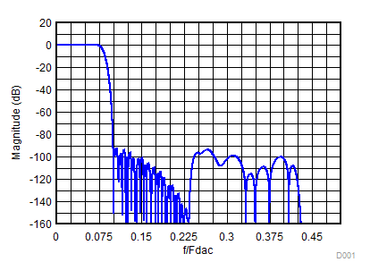
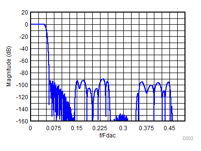
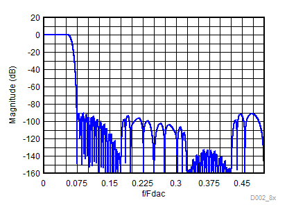
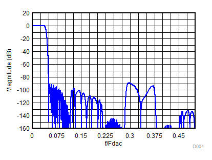
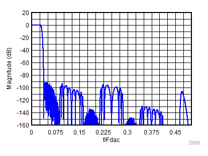
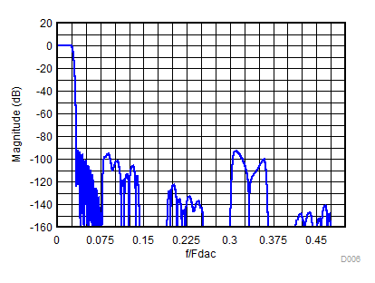
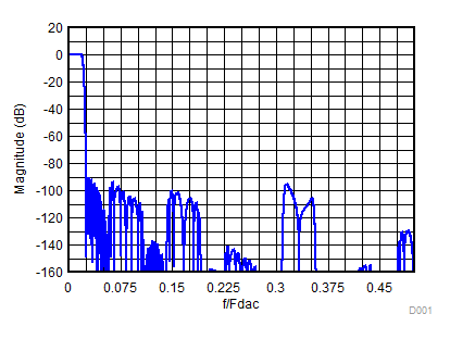
The FIR filter coefficients are shown in Table 7-35 The FIR filters are design with a passband BW of 0.4 x fINPUT, a stopband attenuation of 90 dBc and ripple of < 0.001 dB. The composite frequency response for each interpolation factor are shown in Figure 7-14 to Figure 7-21.

| tap | FIR0 | FIR1 | LPFIR0_5X | FIR2 | LPFIR0_3X | FIR3 | LPFIR1_3X | INVSINC |
|---|---|---|---|---|---|---|---|---|
| 1 | 6 | -12 | -6 | 29 | -14 | 3 | 25 | 1 |
| 2 | 0 | 0 | -22 | 0 | -61 | 0 | 88 | -4 |
| 3 | -19 | 84 | -51 | -214 | -125 | -25 | 22 | 13 |
| 4 | 0 | 0 | -89 | 0 | -95 | 0 | -576 | -50 |
| 5 | 47 | -336 | -117 | 1209 | 181 | 150 | -1764 | 592 |
| 6 | 0 | 0 | -106 | 2048 | 681 | 256 | -2263 | -50 |
| 7 | -100 | 1006 | -18 | 1209 | 972 | 150 | 491 | 13 |
| 8 | 0 | 0 | 171 | 0 | 347 | 0 | 8139 | -4 |
| 9 | 192 | -2691 | 449 | -214 | -1475 | -25 | 18625 | 1 |
| 10 | 0 | 0 | 745 | 0 | -3519 | 0 | 26365 | |
| 11 | -342 | 10141 | 930 | 29 | -3528 | 3 | 26365 | |
| 12 | 0 | 16384 | 841 | 707 | 18625 | |||
| 13 | 572 | 10141 | 338 | 9337 | 8139 | |||
| 14 | 0 | 0 | -618 | 19445 | 491 | |||
| 15 | -914 | -2691 | -1892 | 26299 | -2263 | |||
| 16 | 0 | 0 | -3147 | 26299 | -1764 | |||
| 17 | 1409 | 1006 | -3872 | 19445 | -576 | |||
| 18 | 0 | 0 | -3500 | 9337 | 22 | |||
| 19 | -2119 | -336 | -1564 | 707 | 88 | |||
| 20 | 0 | 0 | 2121 | -3528 | 25 | |||
| 21 | 3152 | 84 | 7336 | -3519 | ||||
| 22 | 0 | 0 | 13430 | -1475 | ||||
| 23 | -4729 | -12 | 19426 | 347 | ||||
| 24 | 0 | 24231 | 972 | |||||
| 25 | 7420 | 26904 | 681 | |||||
| 26 | 0 | 26904 | 181 | |||||
| 27 | -13334 | 24231 | -95 | |||||
| 28 | 0 | 19426 | -125 | |||||
| 29 | 41527 | 13430 | -61 | |||||
| 30 | 65536 | 7336 | -14 | |||||
| 31 | 41527 | 2121 | ||||||
| 32 | 0 | -1564 | ||||||
| 33 | -13334 | -3500 | ||||||
| 34 | 0 | -3872 | ||||||
| 35 | 7420 | -3147 | ||||||
| 36 | 0 | -1892 | ||||||
| 37 | -4729 | -618 | ||||||
| 38 | 0 | 338 | ||||||
| 39 | 3152 | 841 | ||||||
| 40 | 0 | 930 | ||||||
| 41 | -2119 | 745 | ||||||
| 42 | 0 | 449 | ||||||
| 43 | 1409 | 171 | ||||||
| 44 | 0 | -18 | ||||||
| 45 | -914 | -106 | ||||||
| 46 | 0 | -117 | ||||||
| 47 | 572 | -89 | ||||||
| 48 | 0 | -51 | ||||||
| 49 | -342 | -22 | ||||||
| 50 | 0 | -6 | ||||||
| 51 | 192 | |||||||
| 52 | 0 | |||||||
| 53 | -100 | |||||||
| 54 | 0 | |||||||
| 55 | 47 | |||||||
| 56 | 0 | |||||||
| 57 | -19 | |||||||
| 58 | 0 | |||||||
| 59 | 6 |