ZHCSG02C September 2016 – January 2017 TPD6S300
PRODUCTION DATA.
- 1 特性
- 2 应用
- 3 说明
- 4 修订历史记录
- 5 Device Comparison Table
- 6 Pin Configuration and Functions
- 7 Specifications
-
8 Detailed Description
- 8.1 Overview
- 8.2 Functional Block Diagram
- 8.3
Feature Description
- 8.3.1 4-Channels of Short-to-VBUS Overvoltage Protection (CC1, CC2, SBU1, SBU2 Pins): 24-VDC Tolerant
- 8.3.2 8-Channels of IEC 61000-4-2 ESD Protection (CC1, CC2, SBU1, SBU2, DP_T, DM_T, DP_B, DM_B Pins)
- 8.3.3 CC1, CC2 Overvoltage Protection FETs 600 mA Capable for Passing VCONN Power
- 8.3.4 CC Dead Battery Resistors Integrated for Handling the Dead Battery Use Case in Mobile Devices
- 8.3.5 3-mm × 3-mm WQFN Package
- 8.4 Device Functional Modes
- 9 Application and Implementation
- 10Power Supply Recommendations
- 11Layout
- 12器件和文档支持
- 13机械、封装和可订购信息
9 Application and Implementation
NOTE
Information in the following applications sections is not part of the TI component specification, and TI does not warrant its accuracy or completeness. TI’s customers are responsible for determining suitability of components for their purposes. Customers should validate and test their design implementation to confirm system functionality.
9.1 Application Information
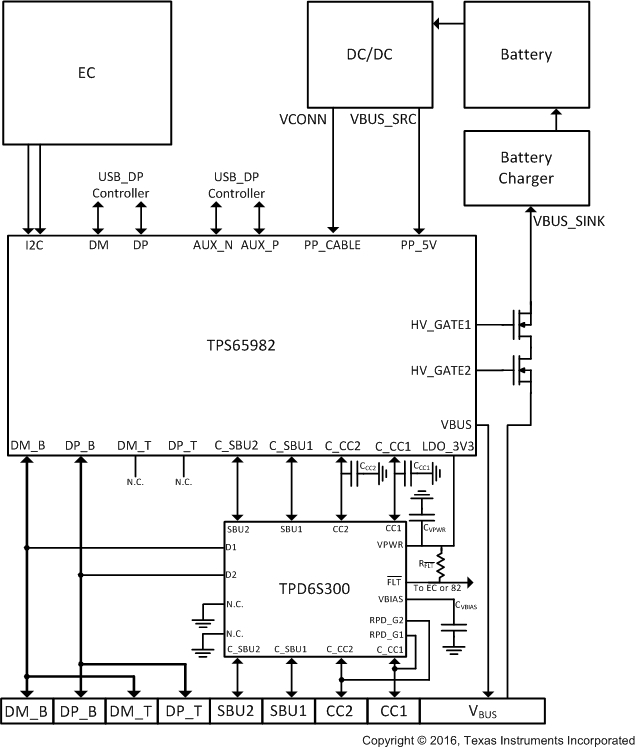
The TPD6S300 provides 4-channels of Short-to-VBUS overvoltage protection for the CC1, CC2, SBU1, and SBU2 pins of the USB Type-C connector, and 8-channels of IEC ESD protection for the CC1, CC2, SBU1, SBU2, DP_T, DM_T, DP_B, DM_B pins of the USB Type-C connector. Care must be taken to insure that the TPD6S300 provides adequate system protection as well as insuring that proper system operation is maintained. The following application example explains how to properly design the TPD6S300 into a USB Type-C system.
9.2 Typical Application
 Figure 30. TPD6S300 Typical Application Diagram
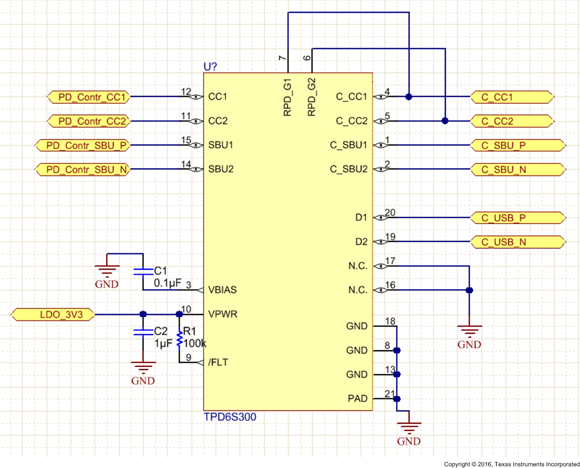
 Figure 31. TPD6S300 Reference Schematic
9.2.1 Design Requirements
In this application example we study the protection requirements for a full-featured USB Type-C DRP Port, fully equipped with USB-PD, USB2.0, USB3.0, Display Port, and 100 W charging. The TPS65982 is used to easily enable a full-featured port with a single chip solution. In this application, all the pins of the USB Type-C connector are utilized. Both the CC and SBU pins are susceptible to shorting to the VBUS pin. With 100 W charging, VBUS operates at 20 V, requiring the CC and SBU pins to tolerate 20-VDC. Additionally, the CC, SBU, and USB2.0 pins require IEC system level ESD protection. With these protection requirements present for the USB Type-C connector, the TPD6S300 is utilized. The TPD6S300 is a single chip solution that provides all the required protection for the low speed and USB2.0 pins in the USB Type-C connector.
Table 2 lists the TPD6S300 design parameters.
Table 2. Design Parameters
| DESIGN PARAMETER | EXAMPLE VALUE |
|---|---|
| VBUS nominal operating voltage | 20 V |
| Short-to-VBUS tolerance for the CC and SBU pins | 24 V |
| VBIAS nominal capacitance | 0.1 µF |
| Dead battery charging | 100 W |
| Maximum ambient temperature requirement | 85°C |
9.2.2 Detailed Design Procedure
9.2.2.1 VBIAS Capacitor Selection
As noted in the Recommended Operating Conditions table, a minimum of 35-VBUS rated capacitor is required for the VBIAS pin, and a 50-VBUS capacitor is recommended. The VBIAS capacitor is in parallel with the central IEC diode clamp integrated inside the TPD6S300. A forward biased hiding diode connects the VBIAS pin to the C_CCx and C_SBUx pins. Therefore, when a Short-to-VBUS event occurs at 20 V, 20-VBUS minus a forward biased diode drop is exposed to the VBIAS pin. Additionally, during the short-to-VBUS event, ringing can occur almost double the settling voltage of 20 V, allowing a potential 40 V to be exposed to the C_CCx and C_SBUx pins. However, the internal IEC clamps limit the voltage exposed to the C_CCx and C_SBUx pins to around 30 V. Therefore, at least 35-VBUS capacitor is required to insure the VBIAS capacitor does not get destroyed during Short-to-VBUS events.
A 50-V, X7R capacitor is recommended, however. This is to further improve the derating performance of the capacitors. When the voltage across a real capacitor is increased, its capacitance value derates. The more the capacitor derates, the greater than 2x ringing can occur in the short-to-VBUS RLC circuit. 50-V X7R capacitors have great derating performance, allowing for the best short-to-VBUS performance of the TPD6S300.
Additionally, the VBIAS capacitor helps pass IEC 61000-4-2 ESD strikes. The more capacitance present, the better the IEC performance. So the less the VBIAS capacitor derates, the better the IEC performance. Table 3 shows real capacitors recommended to achieve the best performance with the TPD6S300.
Table 3. Design Parameters
| CAPACITOR SIZE | PART NUMBER |
|---|---|
| 0402 | CC0402KRX7R9BB104 |
| 0603 | GRM188R71H104KA93D |
9.2.2.2 Dead Battery Operation
For this application, we want to support 100-W dead battery operation; when the laptop is out of battery, we still want to charge the laptop at 20 V and 5 A. This means that the USB PD Controller must receive power in dead battery mode. The TPS65982 has its own built in LDO in order to supply the TPS65982 power from VBUS in a dead battery condition. The TPS65982 can also provide power to its flash during this condition through its LDO_3V3 pin.
The TPD6S300s OVP FETs remain OFF when it is unpowered in order to insure in a dead battery situation proper protection is still provided to the PD controller in the system, in this case the TPS65982. However, when the OVP FETs are OFF, this isolates the TPS65982s dead battery resistors from the USB Type-C ports CC pins. A USB Type-C power adaptor must see the RD pull-down dead battery resistors on the CC pins or it does not provide power on VBUS. Since the TPS65982s dead battery resistors are isolated from the USB Type-C connector's CC pins, the TPD6S300s built in dead battery resistors must be connected. Short the RPD_G1 pin to the C_CC1 pin, and short the RPD_G2 pin to the C_CC2 pin.
Once the power adaptor sees the TPD6S300s dead battery resistors, it applies 5 V on the VBUS pin. This provides power to the TPS65982, turning the PD controller on, and allowing the battery to begin to charge. However, this application requires 100 W charging in dead battery mode, so VBUS at 20 V and 5 A is required. USB PD negotiation is required to accomplish this, so the TPS65982 needs to be able to communicate on the CC pins. This means the TPD6S3000 needs to be turned on in dead battery mode as well so the TPS65982s PD controller can be exposed to the CC lines. To accomplish this, it is critical that the TPD6S300 is powered by the TPS65982s internal LDO, the LDO_3V3 pin. This way, when the TPS65982 receives power on VBUS, the TPD6S300 is turned on simultaneously.
It is critical that the TPS65982s dead battery resistors are also connected to its CC pins for dead battery operation. Short the TPS65982s RPD_G1 pin to its C_CC1 pin, and its RPD_G2 pin to its C_CC2 pin. It is critical that the TPS65982s dead battery resistors are present; once the TPD6S300 receives power, removes its dead battery resistors and turns on its OVP FETs, RD pull-down resistors must be present on the CC line in order to guarantee the power adaptor stays connected. If RD is not present and the voltage on CC changes for more than 10 ms, the power adaptor interprets this as a disconnect and remove VBUS.
Also, it is important that the TPS65982s dead battery resistors are present so it properly boots up in dead battery operation with the correct voltages on its CC pins.
Once this process has occurred, the TPS65982 can start negotiating with the power adaptor through USB PD for higher power levels, allowing 100-W operation in dead battery mode.
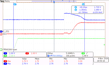
For more information on the TPD6S300 dead battery operation, see the CC Dead Battery Resistors Integrated for Handling the Dead Battery Use Case in Mobile Devices section of the datasheet. Also, see Figure 32 for a waveform of the CC line when the TPD6S300 is turning on and exposing the TPS65982s dead battery resistors to the USB Type-C connector.
9.2.2.3 CC Line Capacitance
USB PD has a specification for the total amount of capacitance that is required for proper USB PD BMC operation on the CC lines. The specification from section 5.8.6 of the USB PD Specification is given below in Table 4.
Table 4. USB PD cReceiver Specification
| NAME | DESCRIPTION | MIN | MAX | UNIT | COMMENT |
|---|---|---|---|---|---|
| cReceiver | CC receiver capacitance | 200 | 600 | pF | The DFP or UFP system shall have capacitance within this range when not transmitting on the line |
Therefore, the capacitance on the CC lines must stay in between 200 pF and 600 pF when USB PD is being used. Therefore, the combination of capacitances added to the system by the TPS65982, the TPD6S300, and any external capacitor must fall within these limits. Table 5 shows the analysis involved in choosing the correct external CC capacitor for this system, and shows that an external CC capacitor is required.
Table 5. CC Line Capacitor Calculation
| CC Capacitance | MIN | MAX | UNIT | COMMENT |
|---|---|---|---|---|
| CC line target capacitance | 200 | 600 | pF | From the USB PD Specification section |
| TPS65982 capacitance | 70 | 120 | pF | From the TPS65982 Datasheet |
| TPD6S300 capacitance | 60 | 120 | pF | From the table. |
| Proposed capacitor GRM033R71E221KA01D | 110 | 330 | pF | CAP, CERM, 220 pF, 25 V, ±10%, X7R, 0201 (For min and max, assume ±50% capacitance change with temperature and voltage derating to be overly conservative) |
| TPS65982 + TPD6S300 + GRM033R71E221KA01D | 240 | 570 | pF | Meets USB PD cReceiver specification |
9.2.2.4 Additional ESD Protection on CC and SBU Lines
If additional IEC ESD protection is desired to be placed on either the CC or SBU lines, it is important that high-voltage ESD protection diodes be used. The maximum DC voltage that can be seen in USB PD is 21-VBUS, with 21.5 V allowed during voltage transitions. Therefore, an ESD protection diode must have a reverse stand off voltage higher than 21.5 V in order to guarantee the diode does not breakdown during a short-to-VBUS event and have large amounts of current flowing through it indefinitely, destroying the diode. A reverse stand off voltage of 24 V is recommended to give margin above 21.5 V in case USB Type-C power adaptors are released in the market which break the USB Type-C specification.
Furthermore, due to the fact that the Short-to-VBUS event applies a DC voltage to the CC and SBU pins, a deep-snap back diode cannot be used unless its minimum trigger voltage is above 42 V. During a Short-to-VBUS event, RLC ringing of up to 2x the settling voltage can be exposed to CC and SBU, allowing for up to 42 V to be exposed. Furthermore, if any capacitor derates on the CC or SBU line, greater than 2x ringing can occur. Since this ringing is hard to bound, it is recommended to not use deep-snap back diodes. If the diode triggers during the short-to-VBUS hot-plug event, it begins to operate in is conduction region. With a 20-VBUS source present on the CC or SBU line, this allows the diode to conduct indefinitely, destroying the diode.
9.2.2.5 FLT Pin Operation
The FLT and OVP FET have specific timing parameters to allow different benefits depending on how the system designer desires the system to respond to a Short-to-VBUS event.
Once a Short-to-VBUS occurs on the C_CCx or C_SBUx pins, the FLT pin is asserted in 20 µs (typical) so the PD controller can be notified quickly. If VBUS is being shorted to CC or SBU, it is recommended to respond to the event by forcing a detach in the USB PD controller to remove VBUS from the port. Although the USB Type-C port using the TPD6S300 is not damaged, as the TPD6S300 provides protection from these events, the other device connected through the USB Type-C Cable or any active circuitry in the cable can be damaged. Although shutting the VBUS off through a detach does not guarantee it stops the other device or cable from being damaged, it can mitigate any high current paths from causing further damage after the initial damage takes place. Additionally, even if the active cable or other device does have proper protection, the short-to-VBUS event may corrupt a configuration in an active cable or in the other PD controller, so it is best to detach and reconfigure the port.
For UFP's, the TPD6S300 automatically forces a detach, removing the need to use the FLT pin if the only response required by your system during a short-to-VBUS event is forcing a detach on the port. The TPD6S300 keeps its CC OVP FET OFF for at least 21 ms after a Short-to-VBUS event occurs, causing the CC line voltage to change from is configuration value for more than 20 ms, forcing the PD controllers to detach. For DFPs, this operation cannot be guaranteed because of the parasitic diode in the OVP FET from CCx to C_CCx and from SBUx to C_SBUx. Therefore for DFPs, using the FLT pin recommended. For our application using the TPS65982 as a DRP, using the FLT pin is recommended.
9.2.2.6 How to Connect Unused Pins
If either the RPD_Gx pins or any of the Dx pins are unused in a design, they must be connected to GND.
9.2.3 Application Curves

