ZHCSG16A January 2017 – May 2017 LMK61E0M
PRODUCTION DATA.
- 1 特性
- 2 应用
- 3 说明
- 4 修订历史记录
- 5 Pin Configuration and Functions
-
6 Specifications
- 6.1 Absolute Maximum Ratings
- 6.2 ESD Ratings
- 6.3 Recommended Operating Conditions
- 6.4 Thermal Information
- 6.5 Electrical Characteristics - Power Supply
- 6.6 3.3-V LVCMOS Output Characteristics
- 6.7 OE Input Characteristics
- 6.8 ADD Input Characteristics
- 6.9 Frequency Tolerance Characteristics
- 6.10 Frequency Margining Characteristics
- 6.11 Power-On/Reset Characteristics (VDD)
- 6.12 I2C-Compatible Interface Characteristics (SDA, SCL)
- 6.13 Other Characteristics
- 6.14 PLL Clock Output Jitter Characteristics
- 6.15 Additional Reliability and Qualification
- 6.16 Typical Characteristics
- 7 Parameter Measurement Information
-
8 Detailed Description
- 8.1 Overview
- 8.2 Functional Block Diagram
- 8.3
Feature Description
- 8.3.1 Device Block-Level Description
- 8.3.2 Device Configuration Control
- 8.3.3 Register File Reference Convention
- 8.3.4 Configuring the PLL
- 8.3.5 Integrated Oscillator
- 8.3.6 Reference Divider and Doubler
- 8.3.7 Phase Frequency Detector
- 8.3.8 Feedback Divider (N)
- 8.3.9 Fractional Engine
- 8.3.10 Charge Pump
- 8.3.11 Loop Filter
- 8.3.12 VCO Calibration
- 8.3.13 High-Speed Output Divider
- 8.3.14 High-Speed Clock Output
- 8.3.15 Device Status
- 8.4 Device Functional Modes
- 8.5 Programming
- 8.6
Register Maps
- 8.6.1
Register Descriptions
- 8.6.1.1 VNDRID_BY1 Register; R0
- 8.6.1.2 VNDRID_BY0 Register; R1
- 8.6.1.3 PRODID Register; R2
- 8.6.1.4 REVID Register; R3
- 8.6.1.5 SLAVEADR Register; R8
- 8.6.1.6 EEREV Register; R9
- 8.6.1.7 DEV_CTL Register; R10
- 8.6.1.8 XO_CAPCTRL_BY1 Register; R16
- 8.6.1.9 XO_CAPCTRL_BY0 Register; R17
- 8.6.1.10 CMOSCTL Register; R20
- 8.6.1.11 DIFFCTL Register; R21
- 8.6.1.12 OUTDIV_BY1 Register; R22
- 8.6.1.13 OUTDIV_BY0 Register; R23
- 8.6.1.14 RDIVCMOSCTL Register; R24
- 8.6.1.15 PLL_NDIV_BY1 Register; R25
- 8.6.1.16 PLL_NDIV_BY0 Register; R26
- 8.6.1.17 PLL_FRACNUM_BY2 Register; R27
- 8.6.1.18 PLL_FRACNUM_BY1 Register; R28
- 8.6.1.19 PLL_FRACNUM_BY0 Register; R29
- 8.6.1.20 PLL_FRACDEN_BY2 Register; R30
- 8.6.1.21 PLL_FRACDEN_BY1 Register; R31
- 8.6.1.22 PLL_FRACDEN_BY0 Register; R32
- 8.6.1.23 PLL_MASHCTRL Register; R33
- 8.6.1.24 PLL_CTRL0 Register; R34
- 8.6.1.25 PLL_CTRL1 Register; R35
- 8.6.1.26 PLL_LF_R2 Register; R36
- 8.6.1.27 PLL_LF_C1 Register; R37
- 8.6.1.28 PLL_LF_R3 Register; R38
- 8.6.1.29 PLL_LF_C3 Register; R39
- 8.6.1.30 PLL_CALCTRL Register; R42
- 8.6.1.31 NVMSCRC Register; R47
- 8.6.1.32 NVMCNT Register; R48
- 8.6.1.33 NVMCTL Register; R49
- 8.6.1.34 MEMADR Register; R51
- 8.6.1.35 NVMDAT Register; R52
- 8.6.1.36 RAMDAT Register; R53
- 8.6.1.37 NVMUNLK Register; R56
- 8.6.1.38 INT_LIVE Register; R66
- 8.6.1.39 SWRST Register; R72
- 8.6.1
Register Descriptions
- 9 Application and Implementation
- 10Power Supply Recommendations
- 11Layout
- 12器件和文档支持
- 13机械、封装和可订购信息
11 Layout
11.1 Layout Guidelines
Ensured Thermal Reliability, Best Practices for Signal Integrity and Recommended Solder Reflow Profile provide recommendations for board layout, solder reflow profile and power supply bypassing when using LMK61E0 to ensure good thermal and electrical performance and overall signal integrity of entire system.
11.1.1 Ensured Thermal Reliability
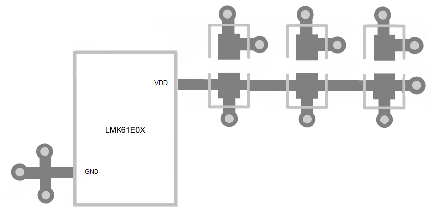
The LMK61E0 is a high performance device. Therefore careful attention must be paid to device configuration and printed-circuit board (PCB) layout with respect to power consumption. The ground pin needs to be connected to the ground plane of the PCB through three vias or more, as shown in Figure 16, to maximize thermal dissipation out of the package.
Equation 4 describes the relationship between the PCB temperature around the LMK61E0 and its junction temperature.
where
- TB: PCB temperature around the LMK61E0
- TJ: Junction temperature of LMK61E0
- ΨJB: Junction-to-board thermal resistance parameter of LMK61E0 (36.7°C/W without airflow)
- P: On-chip power dissipation of LMK61E0
To ensure that the maximum junction temperature of LMK61E0 is below 115°C, it can be calculated that the maximum PCB temperature without airflow should be at 93°C or below when the device is optimized for best performance resulting in maximum on-chip power dissipation of 0.6 W.
11.1.2 Best Practices for Signal Integrity
For best electrical performance and signal integrity of entire system with LMK61E0, TI recommends routing vias into decoupling capacitors and then into the LMK61E0. TI also recommends increasing the via count and width of the traces wherever possible. These steps ensure lowest impedance and shortest path for high-frequency current flow. Figure 16 shows the layout recommendation for LMK61E0.
11.1.3 Recommended Solder Reflow Profile
TI also recommends following the solder paste supplier's recommendations to optimize flux activity and to achieve proper melting temperatures of the alloy within the guidelines of J-STD-20. It is preferable for the LMK61E0 to be processed with the lowest peak temperature possible while also remaining below the components peak temperature rating as listed on the MSL label. The exact temperature profile would depend on several factors including maximum peak temperature for the component as rated on the MSL label, Board thickness, PCB material type, PCB geometries, component locations, sizes, densities within PCB, as well solder manufactures recommended profile, and capability of the reflow equipment to as confirmed by the SMT assembly operation.
11.2 Layout Example
 Figure 16. LMK61E0 Layout Recommendation for Power Supply and Ground