ZHCSG16A January 2017 – May 2017 LMK61E0M
PRODUCTION DATA.
- 1 特性
- 2 应用
- 3 说明
- 4 修订历史记录
- 5 Pin Configuration and Functions
-
6 Specifications
- 6.1 Absolute Maximum Ratings
- 6.2 ESD Ratings
- 6.3 Recommended Operating Conditions
- 6.4 Thermal Information
- 6.5 Electrical Characteristics - Power Supply
- 6.6 3.3-V LVCMOS Output Characteristics
- 6.7 OE Input Characteristics
- 6.8 ADD Input Characteristics
- 6.9 Frequency Tolerance Characteristics
- 6.10 Frequency Margining Characteristics
- 6.11 Power-On/Reset Characteristics (VDD)
- 6.12 I2C-Compatible Interface Characteristics (SDA, SCL)
- 6.13 Other Characteristics
- 6.14 PLL Clock Output Jitter Characteristics
- 6.15 Additional Reliability and Qualification
- 6.16 Typical Characteristics
- 7 Parameter Measurement Information
-
8 Detailed Description
- 8.1 Overview
- 8.2 Functional Block Diagram
- 8.3
Feature Description
- 8.3.1 Device Block-Level Description
- 8.3.2 Device Configuration Control
- 8.3.3 Register File Reference Convention
- 8.3.4 Configuring the PLL
- 8.3.5 Integrated Oscillator
- 8.3.6 Reference Divider and Doubler
- 8.3.7 Phase Frequency Detector
- 8.3.8 Feedback Divider (N)
- 8.3.9 Fractional Engine
- 8.3.10 Charge Pump
- 8.3.11 Loop Filter
- 8.3.12 VCO Calibration
- 8.3.13 High-Speed Output Divider
- 8.3.14 High-Speed Clock Output
- 8.3.15 Device Status
- 8.4 Device Functional Modes
- 8.5 Programming
- 8.6
Register Maps
- 8.6.1
Register Descriptions
- 8.6.1.1 VNDRID_BY1 Register; R0
- 8.6.1.2 VNDRID_BY0 Register; R1
- 8.6.1.3 PRODID Register; R2
- 8.6.1.4 REVID Register; R3
- 8.6.1.5 SLAVEADR Register; R8
- 8.6.1.6 EEREV Register; R9
- 8.6.1.7 DEV_CTL Register; R10
- 8.6.1.8 XO_CAPCTRL_BY1 Register; R16
- 8.6.1.9 XO_CAPCTRL_BY0 Register; R17
- 8.6.1.10 CMOSCTL Register; R20
- 8.6.1.11 DIFFCTL Register; R21
- 8.6.1.12 OUTDIV_BY1 Register; R22
- 8.6.1.13 OUTDIV_BY0 Register; R23
- 8.6.1.14 RDIVCMOSCTL Register; R24
- 8.6.1.15 PLL_NDIV_BY1 Register; R25
- 8.6.1.16 PLL_NDIV_BY0 Register; R26
- 8.6.1.17 PLL_FRACNUM_BY2 Register; R27
- 8.6.1.18 PLL_FRACNUM_BY1 Register; R28
- 8.6.1.19 PLL_FRACNUM_BY0 Register; R29
- 8.6.1.20 PLL_FRACDEN_BY2 Register; R30
- 8.6.1.21 PLL_FRACDEN_BY1 Register; R31
- 8.6.1.22 PLL_FRACDEN_BY0 Register; R32
- 8.6.1.23 PLL_MASHCTRL Register; R33
- 8.6.1.24 PLL_CTRL0 Register; R34
- 8.6.1.25 PLL_CTRL1 Register; R35
- 8.6.1.26 PLL_LF_R2 Register; R36
- 8.6.1.27 PLL_LF_C1 Register; R37
- 8.6.1.28 PLL_LF_R3 Register; R38
- 8.6.1.29 PLL_LF_C3 Register; R39
- 8.6.1.30 PLL_CALCTRL Register; R42
- 8.6.1.31 NVMSCRC Register; R47
- 8.6.1.32 NVMCNT Register; R48
- 8.6.1.33 NVMCTL Register; R49
- 8.6.1.34 MEMADR Register; R51
- 8.6.1.35 NVMDAT Register; R52
- 8.6.1.36 RAMDAT Register; R53
- 8.6.1.37 NVMUNLK Register; R56
- 8.6.1.38 INT_LIVE Register; R66
- 8.6.1.39 SWRST Register; R72
- 8.6.1
Register Descriptions
- 9 Application and Implementation
- 10Power Supply Recommendations
- 11Layout
- 12器件和文档支持
- 13机械、封装和可订购信息
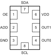
5 Pin Configuration and Functions
SIA Package
8-Pin QFM
Top View

Pin Functions
| PIN | I/O | DESCRIPTION | |
|---|---|---|---|
| NAME | NO. | ||
| POWER | |||
| GND | 3 | Ground | Device Ground. |
| VDD | 6 | Power | 3.3-V Power Supply. |
| OUTPUT BLOCK | |||
| OUT0, OUT1 | 4, 5 | Output | 3.3-V LVCMOS Output Pair (Outputs can be individually set to same polarity, opposite polarity, or tri-state) in LMK61E0M. By default, OUT0 is enabled and OUT1 is disabled and set at high impedance on power-up. |
| DIGITAL CONTROL / INTERFACES | |||
| ADD | 2 | LVCMOS | When left open, LSB of I2C slave address is set to 01. When tied to VDD, LSB of I2C slave address is set to 11. When tied to GND, LSB of I2C slave address is set to 00. |
| OE | 1 | LVCMOS | Output Enable (internal pullup). In LMK61E0M, when set to low, output on OUT0 is disabled and set at high impedance. |
| SCL | 8 | LVCMOS | I2C Serial Clock (open-drain). Requires an external pullup resistor to VDD. |
| SDA | 7 | LVCMOS | I2C Serial Data (bi-directional, open-drain). Requires an external pullup resistor to VDD. |