ZHCSG23A March 2017 – February 2018 LM25141-Q1
PRODUCTION DATA.
- 1 特性
- 2 应用
- 3 说明
- 4 修订历史记录
- 5 Pin Configuration and Functions
- 6 Specifications
-
7 Detailed Description
- 7.1 Overview
- 7.2 Functional Block Diagram
- 7.3
Feature Description
- 7.3.1 High Voltage Start-Up Regulator
- 7.3.2 VCC Regulator
- 7.3.3 Oscillator
- 7.3.4 Synchronization
- 7.3.5 Frequency Dithering (Spread Spectrum)
- 7.3.6 Enable
- 7.3.7 Power Good
- 7.3.8 Output Voltage
- 7.3.9 Current Sense
- 7.3.10 DCR Current Sensing
- 7.3.11 Error Amplifier and PWM Comparator
- 7.3.12 Slope Compensation
- 7.3.13 Hiccup Mode Current Limiting
- 7.3.14 Standby Mode
- 7.3.15 Soft Start
- 7.3.16 Diode Emulation
- 7.3.17 High- and Low-Side Drivers
-
8 Application and Implementation
- 8.1 Application Information
- 8.2 Typical Application
- 9 Power Supply Recommendations
- 10Layout
- 11器件和文档支持
- 12机械、封装和可订购信息
7.3.3 Oscillator
The LM25141-Q1 has an internal trimmed oscillator with two frequency options: 2.2 MHz, or 440 kHz. With the OSC pin connected to VDDA the oscillator frequency is 2.2 MHz. With the OSC pin grounded, the oscillator frequency is 440 kHz. The state of the OSC pin is read and latched during VCC power-up and cannot be changed until VCC drops below the VCC(UVLO) threshold.
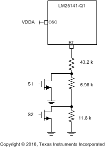
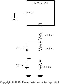
The oscillator frequency can be modulated up or down from the nominal oscillator frequency (2.2 MHz or 440 kHz) on demand by connecting a resistor from the RT pin to ground (refer to Figure 19). To disable the frequency modulation option, the RT pin can be grounded or left open. If the RT pin is connected to ground during power-up the frequency modulation option is latch-off and cannot be changed unless VCC is allowed to drop below the VCC(UVLO) threshold. If the RT pin is left open during power-up the frequency modulation option will be disabled, but it can be enabled at a later time by switching in a valid RT resistor. When the frequency modulation option is disabled, the LM25141-Q1 operates at the internal oscillator frequency (2.2 MHz or 440 kHz).
On power up, after soft start is complete and the output voltage is in regulation, a 16-µs timer is initiated. If a valid RT resistor is connected, the LM25141-Q1 switches to the frequency set by the RT resistor n the completion of the 16-µs time delay.
The modulation range for 2.2 MHz is 1.8 MHz to 2.53 MHz (refer to Table 1). If an RT resistor value > 95 kΩ (typical) is placed on the RT pin, the LM25141-Q1 controller assumes that the RT pin is open and will use the internal oscillator. If an RT resistor < 27 kΩ (typical) is connected, the controller uses the internal oscillator. To calculate an RT resistor for a specific oscillator frequency, use Equation 1 for the 2.2-MHz frequency range or Equation 2 for the 440-kHz frequency range.

where
- RT is kΩ and FSW is in MHz

where
- RT is in kΩ and FSW is in kHz
Table 1. RT Resistance vs Oscillator Frequency
| S1 | S2 | RT RESISTANCE (TYPICAL) 2.2 MHz | 2.2-MHZ OSCILLATOR RANGE (TYPICAL) | RT RESISTANCE (TYPICAL) 440 kHz | 440-kHz OSCILLATOR RANGE (TYPICAL) |
|---|---|---|---|---|---|
| X | X | > 95 kΩ | Internal Oscillator | > 95 kΩ | Internal Oscillator |
| OFF | OFF | 61.98 kΩTotal | 1.8 MHz | 73.8 kΩTotal | 300 kHz |
| OFF | ON | 50.18 kΩTotal | 2.2 MHz | 50.1 kΩTotal | 440 kHz |
| ON | OFF | 43.2 kΩ | 2.53 MHz | 44.2 kΩ | 500 kHz |
| X | X | < 27 kΩ | Internal Oscillator | < 27 kΩ | Internal Oscillator |
 Figure 19. RT Connection Circuit, 2.2 MHz
 Figure 20. RT Connection Circuit, 440 kHz
An alternative method to modulate the oscillator frequency is to use an analog voltage connected to the RT pin through a resistor. See Figure 21. An analog voltage of 0.0 V to 0.6 V modulates the oscillator frequency between 1.8 MHz to 2.53 MHz (OSC at 2.2 MHz), or 300 kHz to 500 kHz (OSC at 440 kHz). The analog voltage source must be able to sink current.
 Figure 21. Analog Voltage Control of the Oscillator Frequency
When the LM25141-Q1 is in the low IQ standby mode, the controller will set the RT pin to a high impedance state and ignore the RT resistor. After coming out of standby mode, the controller will monitor the RT pin. If a valid resistor is connected, and there have been 16 µs of continuous switching without a zero-crossing event, the LM25141-Q1 switches to the frequency set by the RT resistor.