ZHCSG45B March   2017  – March 2018 LM5113-Q1

PRODUCTION DATA.  

  1. 特性
  2. 应用
  3. 说明
    1.     Device Images
      1.      简化应用示意图
  4. 修订历史记录
  5. Pin Configuration and Functions
    1.     Pin Functions
  6. Specifications
    1. 6.1 Absolute Maximum Ratings
    2. 6.2 ESD Ratings
    3. 6.3 Recommended Operating Conditions
    4. 6.4 Thermal Information
    5. 6.5 Electrical Characteristics
    6. 6.6 Switching Characteristics
    7. 6.7 Typical Characteristics
  7. Detailed Description
    1. 7.1 Overview
    2. 7.2 Functional Block Diagram
    3. 7.3 Feature Description
      1. 7.3.1 Input and Output
      2. 7.3.2 Start-Up and UVLO
      3. 7.3.3 HS Negative Voltage and Bootstrap Supply Voltage Clamping
      4. 7.3.4 Level Shift
    4. 7.4 Device Functional Modes
  8. Application and Implementation
    1. 8.1 Application Information
    2. 8.2 Typical Application
      1. 8.2.1 Design Requirements
      2. 8.2.2 Detailed Design Procedure
        1. 8.2.2.1 VDD Bypass Capacitor
        2. 8.2.2.2 Bootstrap Capacitor
        3. 8.2.2.3 Power Dissipation
      3. 8.2.3 Application Curves
  9. Power Supply Recommendations
  10. 10Layout
    1. 10.1 Layout Guidelines
    2. 10.2 Layout Example
  11. 11器件和文档支持
    1. 11.1 文档支持
      1. 11.1.1 相关文档
    2. 11.2 接收文档更新通知
    3. 11.3 社区资源
    4. 11.4 商标
    5. 11.5 静电放电警告
    6. 11.6 Glossary
  12. 12机械、封装和可订购信息

Typical Characteristics

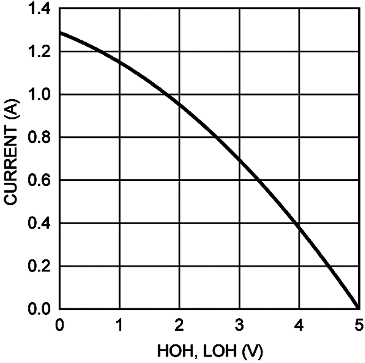
LM5113-Q1 30162905.pngFigure 2. Peak Source Current vs Output Voltage
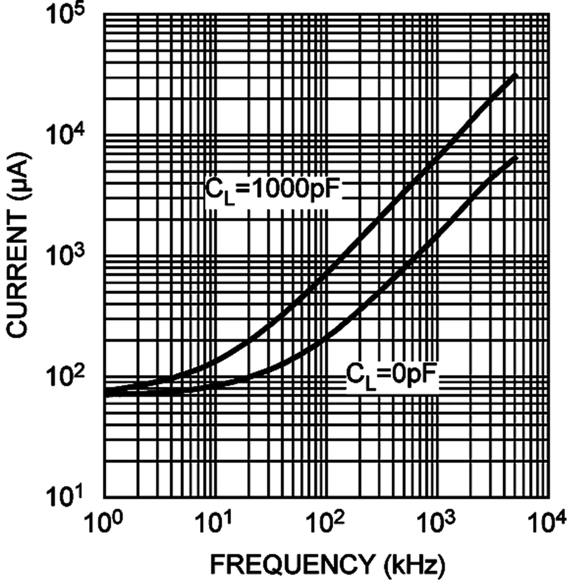
LM5113-Q1 30162907.pngFigure 4. IDDO vs Frequency
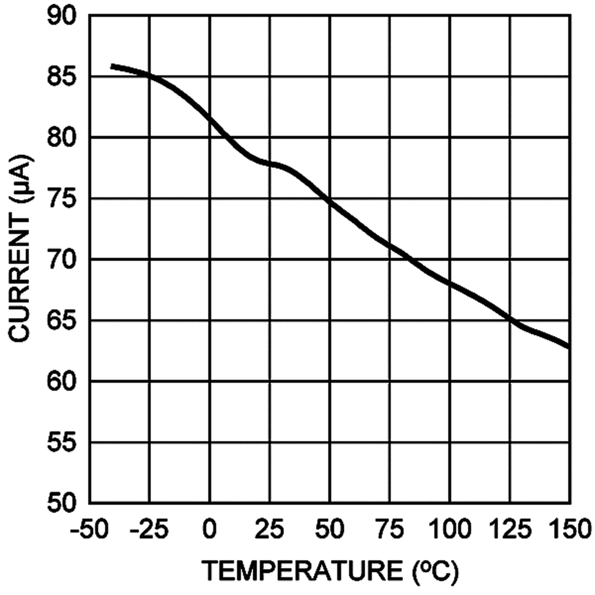
LM5113-Q1 30162909.pngFigure 6. IDD vs Temperature
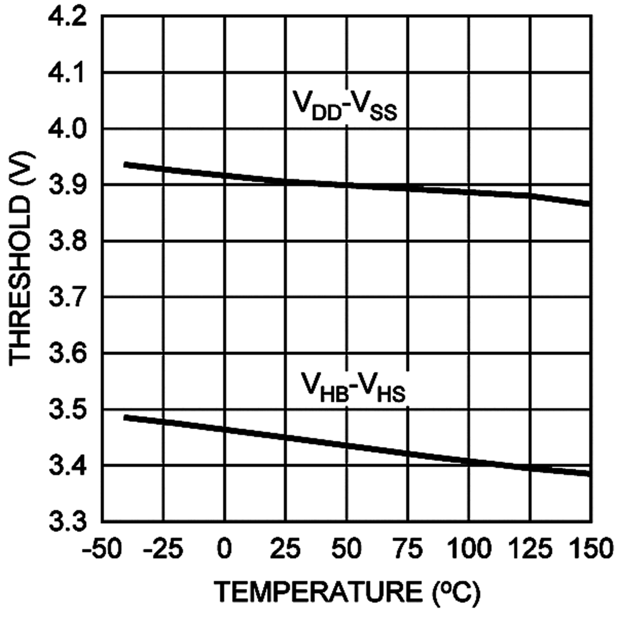
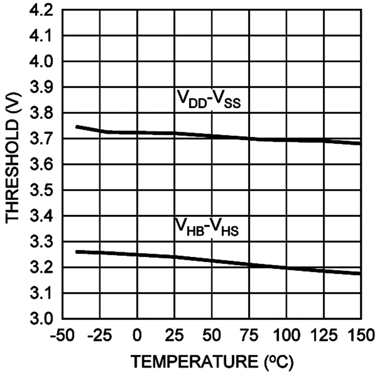
LM5113-Q1 30162911.pngFigure 8. UVLO Rising Thresholds vs Temperature
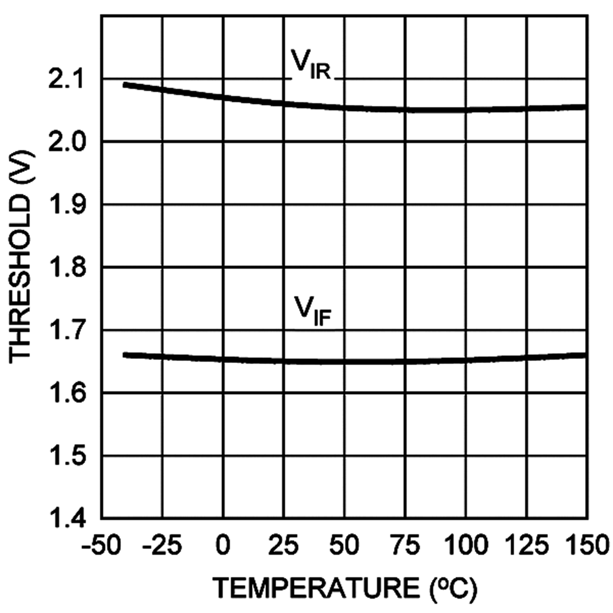
LM5113-Q1 30162913.pngFigure 10. Input Thresholds vs Temperature
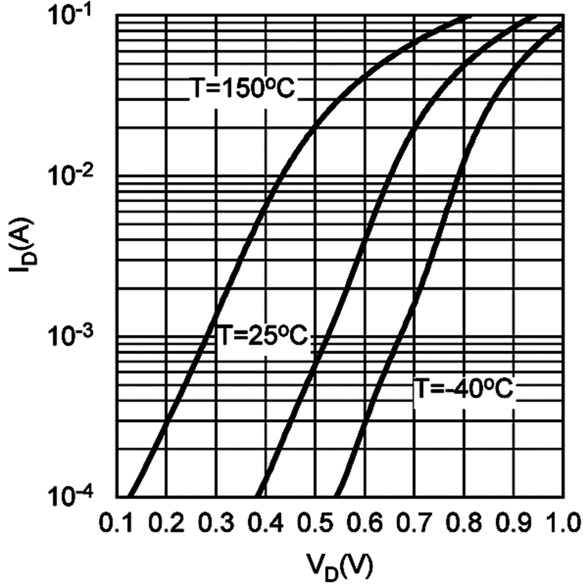
LM5113-Q1 30162915.pngFigure 12. Bootstrap Diode Forward Voltage
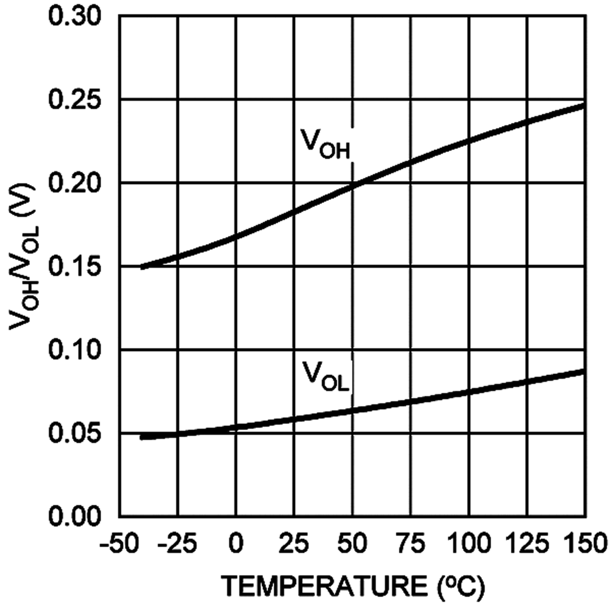
LM5113-Q1 30162917.png
Note: Unless otherwise specified, VDD = VHB = 5 V,
VSS = VHS = 0 V.
Figure 14. LO and HO Gate Drive – High/Low Level
Output Voltage vs Temperature
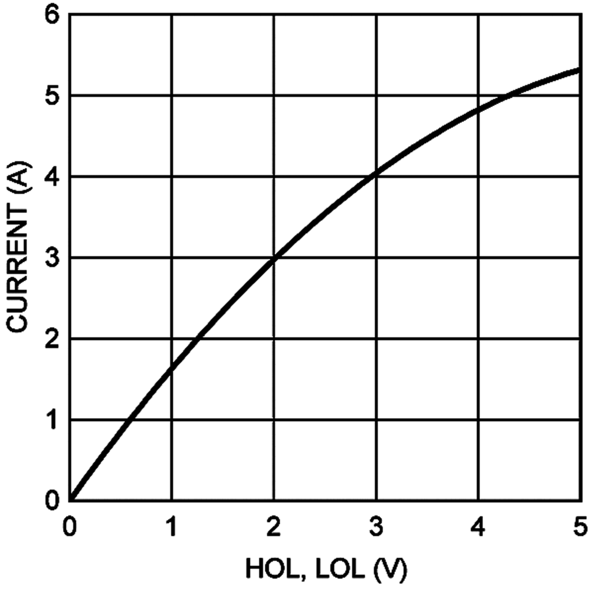
LM5113-Q1 30162906.pngFigure 3. Peak Sink Current vs Output Voltage
LM5113-Q1 30162908.pngFigure 5. IHBO vs Frequency
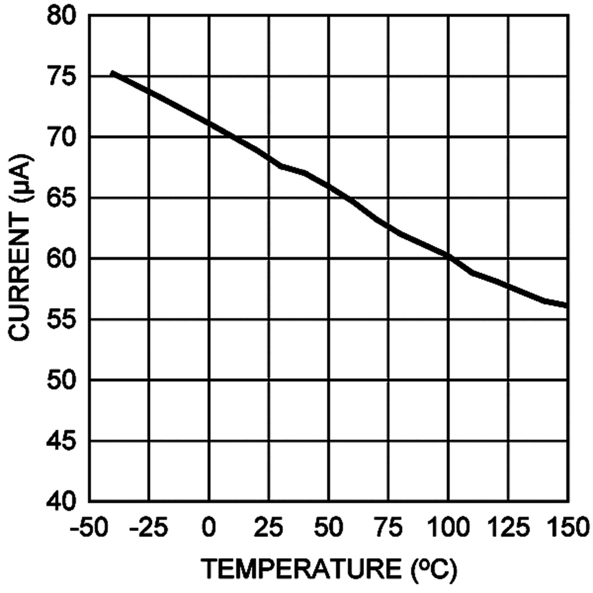
LM5113-Q1 30162910.pngFigure 7. IHB vs Temperature
LM5113-Q1 30162912.pngFigure 9. UVLO Falling Thresholds vs Temperature
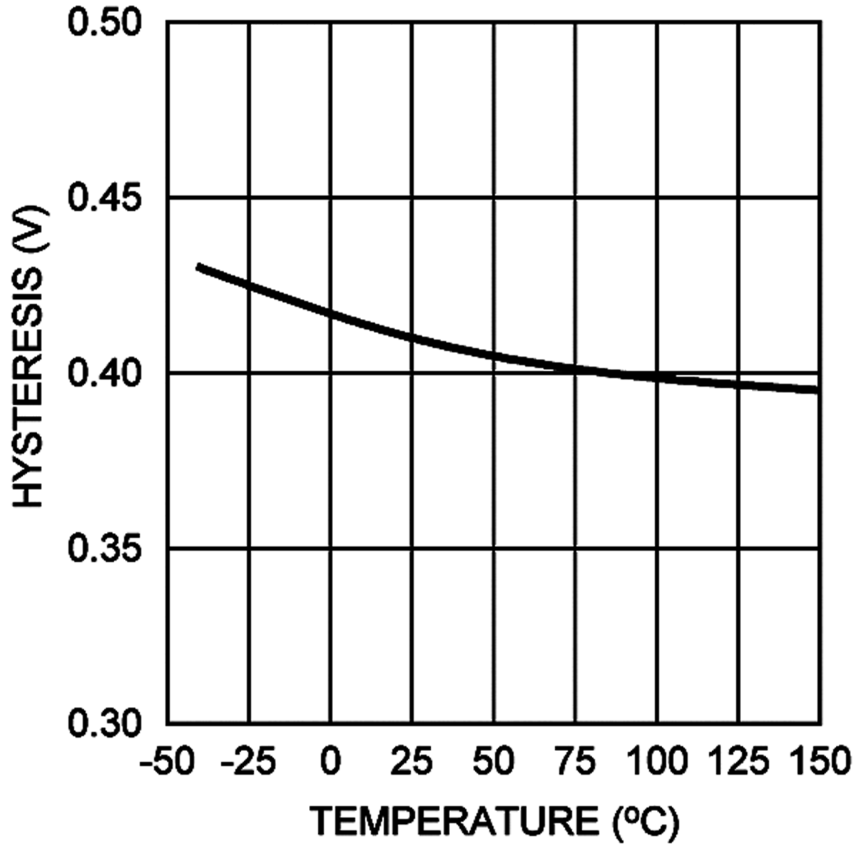
LM5113-Q1 30162914.pngFigure 11. Input Threshold Hysteresis vs Temperature
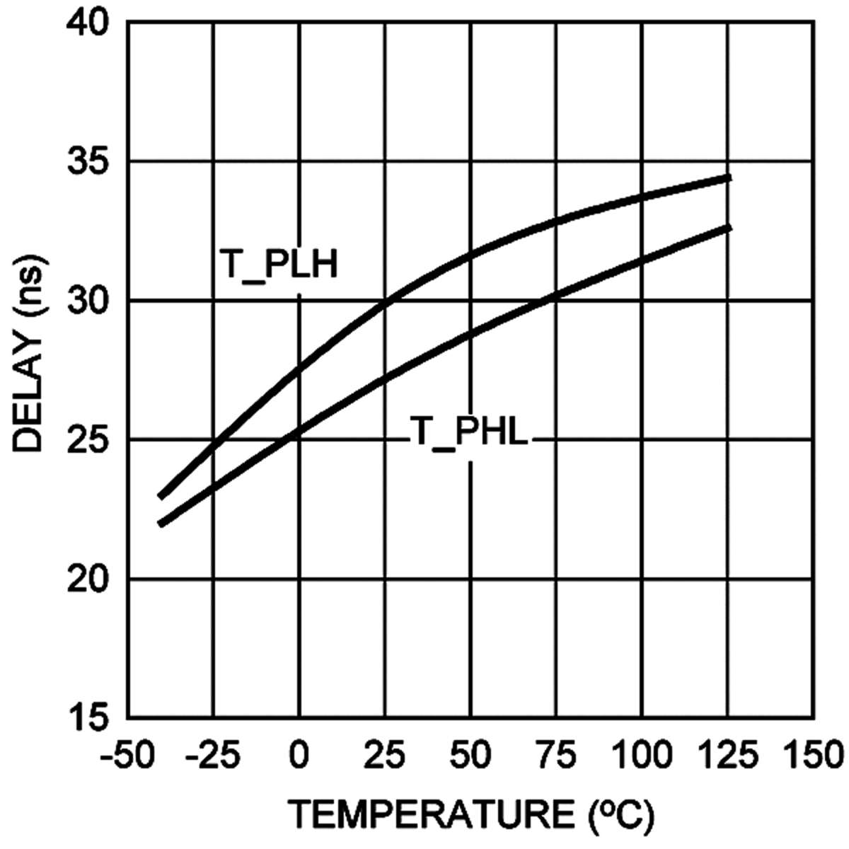
LM5113-Q1 30162916.pngFigure 13. Propagation Delay vs Temperature
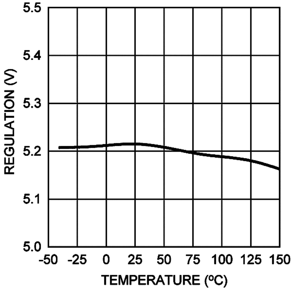
LM5113-Q1 30162918.png
Figure 15. HB Regulation Voltage vs Temperature