ZHCSGA6A February   2017  – June 2017 ADS114S06 , ADS114S08

PRODUCTION DATA.  

  1. 特性
  2. 应用
  3. 说明
    1.     Device Images
      1.      功能方框图
  4. 修订历史记录
  5. Device Family Comparison Table
  6. Pin Configuration and Functions
    1.     Pin Functions
  7. Specifications
    1. 7.1 Absolute Maximum Ratings
    2. 7.2 ESD Ratings
    3. 7.3 Recommended Operating Conditions
    4. 7.4 Thermal Information
    5. 7.5 Electrical Characteristics
    6. 7.6 Timing Characteristics
    7. 7.7 Switching Characteristics
    8. 7.8 Typical Characteristics
  8. Parameter Measurement Information
    1. 8.1 Noise Performance
  9. Detailed Description
    1. 9.1 Overview
    2. 9.2 Functional Block Diagram
    3. 9.3 Feature Description
      1. 9.3.1  Multiplexer
      2. 9.3.2  Low-Noise Programmable Gain Amplifier
        1. 9.3.2.1 PGA Input-Voltage Requirements
        2. 9.3.2.2 PGA Rail Flags
        3. 9.3.2.3 Bypassing the PGA
      3. 9.3.3  Voltage Reference
        1. 9.3.3.1 Internal Reference
        2. 9.3.3.2 External Reference
        3. 9.3.3.3 Reference Buffers
      4. 9.3.4  Clock Source
      5. 9.3.5  Delta-Sigma Modulator
      6. 9.3.6  Digital Filter
        1. 9.3.6.1 Low-Latency Filter
          1. 9.3.6.1.1 Low-Latency Filter Frequency Response
          2. 9.3.6.1.2 Data Conversion Time for the Low-Latency Filter
        2. 9.3.6.2 Sinc3 Filter
          1. 9.3.6.2.1 Sinc3 Filter Frequency Response
          2. 9.3.6.2.2 Data Conversion Time for the Sinc3 Filter
        3. 9.3.6.3 Note on Conversion Time
        4. 9.3.6.4 50-Hz and 60-Hz Line Cycle Rejection
        5. 9.3.6.5 Global Chop Mode
      7. 9.3.7  Excitation Current Sources (IDACs)
      8. 9.3.8  Bias Voltage Generation
      9. 9.3.9  System Monitor
        1. 9.3.9.1 Internal Temperature Sensor
        2. 9.3.9.2 Power Supply Monitors
        3. 9.3.9.3 Burn-Out Current Sources
      10. 9.3.10 Status Register
        1. 9.3.10.1 POR Flag
        2. 9.3.10.2 RDY Flag
        3. 9.3.10.3 PGA Output Voltage Rail Monitors
        4. 9.3.10.4 Reference Monitor
      11. 9.3.11 General-Purpose Inputs and Outputs (GPIOs)
      12. 9.3.12 Low-Side Power Switch
      13. 9.3.13 Cyclic Redundancy Check (CRC)
      14. 9.3.14 Calibration
        1. 9.3.14.1 Offset Calibration
        2. 9.3.14.2 Gain Calibration
    4. 9.4 Device Functional Modes
      1. 9.4.1 Reset
        1. 9.4.1.1 Power-On Reset
        2. 9.4.1.2 RESET Pin
        3. 9.4.1.3 Reset by Command
      2. 9.4.2 Power-Down Mode
      3. 9.4.3 Standby Mode
      4. 9.4.4 Conversion Modes
        1. 9.4.4.1 Continuous Conversion Mode
        2. 9.4.4.2 Single-Shot Conversion Mode
        3. 9.4.4.3 Programmable Conversion Delay
    5. 9.5 Programming
      1. 9.5.1 Serial Interface
        1. 9.5.1.1 Chip Select (CS)
        2. 9.5.1.2 Serial Clock (SCLK)
        3. 9.5.1.3 Serial Data Input (DIN)
        4. 9.5.1.4 Serial Data Output and Data Ready (DOUT/DRDY)
        5. 9.5.1.5 Data Ready (DRDY)
        6. 9.5.1.6 Timeout
      2. 9.5.2 Data Format
      3. 9.5.3 Commands
        1. 9.5.3.1  NOP
        2. 9.5.3.2  WAKEUP
        3. 9.5.3.3  POWERDOWN
        4. 9.5.3.4  RESET
        5. 9.5.3.5  START
        6. 9.5.3.6  STOP
        7. 9.5.3.7  SYOCAL
        8. 9.5.3.8  SYGCAL
        9. 9.5.3.9  SFOCAL
        10. 9.5.3.10 RDATA
        11. 9.5.3.11 RREG
        12. 9.5.3.12 WREG
      4. 9.5.4 Reading Data
        1. 9.5.4.1 Read Data Direct
        2. 9.5.4.2 Read Data by RDATA Command
        3. 9.5.4.3 Sending Commands When Reading Data
      5. 9.5.5 Interfacing with Multiple Devices
    6. 9.6 Register Map
      1. 9.6.1 Configuration Registers
        1. 9.6.1.1  Device ID Register (address = 00h) [reset = xxh]
          1. Table 26. Device ID (ID) Register Field Descriptions
        2. 9.6.1.2  Device Status Register (address = 01h) [reset = 80h]
          1. Table 27. Device Status (STATUS) Register Field Descriptions
        3. 9.6.1.3  Input Multiplexer Register (address = 02h) [reset = 01h]
          1. Table 28. Input Multiplexer (INPMUX) Register Field Descriptions
        4. 9.6.1.4  Gain Setting Register (address = 03h) [reset = 00h]
          1. Table 29. Gain Setting (PGA) Register Field Descriptions
        5. 9.6.1.5  Data Rate Register (address = 04h) [reset = 14h]
          1. Table 30. Data Rate (DATARATE) Register Field Descriptions
        6. 9.6.1.6  Reference Control Register (address = 05h) [reset = 10h]
          1. Table 31. Reference Control (REF) Register Field Descriptions
        7. 9.6.1.7  Excitation Current Register 1 (address = 06h) [reset = 00h]
          1. Table 32. Excitation Current Register 1 (IDACMAG) Register Field Descriptions
        8. 9.6.1.8  Excitation Current Register 2 (address = 07h) [reset = FFh]
          1. Table 33. Excitation Current Register 2 (IDACMUX) Register Field Descriptions
        9. 9.6.1.9  Sensor Biasing Register (address = 08h) [reset = 00h]
          1. Table 34. Sensor Biasing (VBIAS) Register Field Descriptions
        10. 9.6.1.10 System Control Register (address = 09h) [reset = 10h]
          1. Table 35. System Control (SYS) Register Field Descriptions
        11. 9.6.1.11 Reserved Register (address = 0Ah) [reset = 00h]
          1. Table 36. Reserved Register Field Descriptions
        12. 9.6.1.12 Offset Calibration Register 1 (address = 0Bh) [reset = 00h]
          1. Table 37. Offset Calibration Register 1 (OFCAL0) Register Field Descriptions
        13. 9.6.1.13 Offset Calibration Register 2 (address = 0Ch) [reset = 00h]
          1. Table 38. Offset Calibration Register 2 (OFCAL1) Register Field Descriptions
        14. 9.6.1.14 Reserved Register (address = 0Dh) [reset = 00h]
          1. Table 39. Reserved Register Field Descriptions
        15. 9.6.1.15 Gain Calibration Register 1 (address = 0Eh) [reset = 00h]
          1. Table 40. Gain Calibration Register 1 (FSCAL0) Field Descriptions
        16. 9.6.1.16 Gain Calibration Register 2 (address = 0Fh) [reset = 40h]
          1. Table 41. Gain Calibration Register 2 (FSCAL1) Field Descriptions
        17. 9.6.1.17 GPIO Data Register (address = 10h) [reset = 00h]
          1. Table 42. GPIO Data (GPIODAT) Register Field Descriptions
        18. 9.6.1.18 GPIO Configuration Register (address = 11h) [reset = 00h]
          1. Table 43. GPIO Configuration (GPIOCON) Register Field Descriptions
  10. 10Application and Implementation
    1. 10.1 Application Information
      1. 10.1.1 Serial Interface Connections
      2. 10.1.2 Analog Input Filtering
      3. 10.1.3 External Reference and Ratiometric Measurements
      4. 10.1.4 Establishing a Proper Input Voltage
      5. 10.1.5 Unused Inputs and Outputs
      6. 10.1.6 Pseudo Code Example
    2. 10.2 Typical Application
      1. 10.2.1 Design Requirements
      2. 10.2.2 Detailed Design Procedure
        1. 10.2.2.1 Register Settings
      3. 10.2.3 Application Curves
    3. 10.3 Do's and Don'ts
  11. 11Power Supply Recommendations
    1. 11.1 Power Supplies
    2. 11.2 Power-Supply Sequencing
    3. 11.3 Power-On Reset
    4. 11.4 Power-Supply Decoupling
  12. 12Layout
    1. 12.1 Layout Guidelines
    2. 12.2 Layout Example
  13. 13器件和文档支持
    1. 13.1 器件支持
      1. 13.1.1 开发支持
    2. 13.2 文档支持
      1. 13.2.1 相关文档
    3. 13.3 相关链接
    4. 13.4 接收文档更新通知
    5. 13.5 社区资源
    6. 13.6 商标
    7. 13.7 静电放电警告
    8. 13.8 Glossary
  14. 14机械、封装和可订购信息

Voltage Reference

The devices require a reference voltage for operation. The ADS114S0x offers an integrated low-drift 2.5-V reference. For applications that require a different reference voltage value or a ratiometric measurement approach, the ADS114S08 offers two differential reference input pairs (REFP0, REFN0 and REFP1, REFN1). The differential reference inputs allow freedom in the reference common-mode voltage. REFP0 and REFN0 are dedicated reference inputs, whereas REFP1 and REFN1 are shared with inputs AIN6 and AIN7 (respectively) on the ADS114S08. The specified external reference voltage range is 0.5 V to AVDD. The reference voltage is shown in Equation 7, where V(REFPx) and V(REFNx) are the absolute positive and absolute negative reference voltages.

Equation 7. VREF = V(REFPx) – V(REFNx)

The polarity of the reference voltage internal to the ADC must be positive. The magnitude of the reference voltage together with the PGA gain establishes the ADC full-scale differential input range as defined by
FSR = ±VREF / Gain.

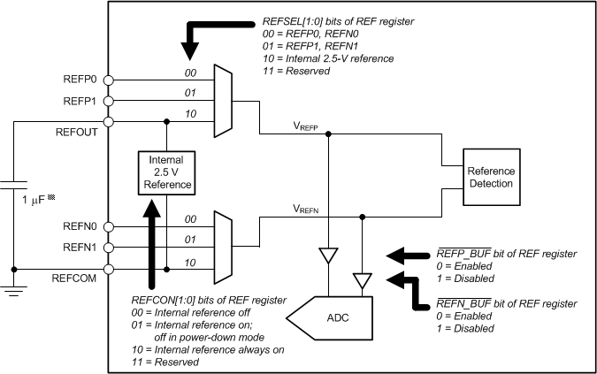
Figure 52 shows the block diagram of the reference multiplexer. The ADC reference multiplexer selects between the internal reference and two external references (REF0 and REF1). The reference multiplexer is programmed with the REFSEL[1:0] bits in the reference control register (05h). By default, the external reference pair REFP0, REFN0 is selected.
ADS114S06 ADS114S08 ai_ref_mux2_sbas660.gif
The internal reference requires a minimum 1-µF capacitor connected from REFOUT to REFCOM.
Figure 52. Reference Multiplexer Block Diagram

The ADC also contains an integrated reference voltage monitor. This monitor provides continuous detection of a low or missing reference during the conversion cycle. The reference monitor flags (FL_REF_L0 and FL_REF_L1) are set in the STATUS byte and described in the Reference Monitor section.