ZHCSGB0B November 2017 – November 2020 LM5145
PRODUCTION DATA
- 1 特性
- 2 应用
- 3 说明
- 4 Revision History
- 5 Description (continued)
- 6 Pin Configuration and Functions
- 7 Specifications
-
8 Detailed Description
- 8.1 Overview
- 8.2 Functional Block Diagram
- 8.3
Feature Description
- 8.3.1 Input Range (VIN)
- 8.3.2 Output Voltage Setpoint and Accuracy (FB)
- 8.3.3 High-Voltage Bias Supply Regulator (VCC)
- 8.3.4 Precision Enable (EN/UVLO)
- 8.3.5 Power Good Monitor (PGOOD)
- 8.3.6 Switching Frequency (RT, SYNCIN)
- 8.3.7 Configurable Soft Start (SS/TRK)
- 8.3.8 Voltage-Mode Control (COMP)
- 8.3.9 Gate Drivers (LO, HO)
- 8.3.10 Current Sensing and Overcurrent Protection (ILIM)
- 8.3.11 OCP Duty Cycle Limiter
- 8.4 Device Functional Modes
-
9 Application and Implementation
- 9.1 Application Information
- 9.2
Typical Applications
- 9.2.1 Design 1 – 20-A High-Efficiency Synchronous Buck Regulator for Telecom Power Applications
- 9.2.2 Design 2 – High Density, 12-V, 10-A Rail With LDO Low-Noise Auxiliary Output for RF Power Applications
- 9.2.3 Design 3 – 150-W, Regulated 24-V Rail for Commercial Drone Applications With Output Voltage Tracking Feature
- 9.2.4 Design 4 – Powering a Multicore DSP From a 24-V or 48-V Rail
- 10Power Supply Recommendations
- 11Layout
- 12Device and Documentation Support
- 13Mechanical, Packaging, and Orderable Information
11.1 Layout Guidelines
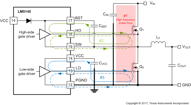
Proper PCB design and layout is important in a high-current, fast-switching circuits (with high current and voltage slew rates) to assure appropriate device operation and design robustness. As expected, certain issues must be considered before designing a PCB layout using the LM5145. The high-frequency power loop of the buck converter power stage is denoted by #1 in the shaded area of Figure 11-1. The topological architecture of a buck converter means that particularly high di/dt current flows in the components of loop 1, and it becomes mandatory to reduce the parasitic inductance of this loop by minimizing its effective loop area. Also important is the gate drive loops of the low-side and high-side MOSFETs, denoted by 2 and 3, respectively, in Figure 11-1.
 Figure 11-1 DC-DC Regulator Ground System With Power Stage and Gate Drive Circuit Switching Loops