ZHCSGD0 June 2017 LM25145
PRODUCTION DATA.
- 1 特性
- 2 应用
- 3 说明
- 4 修订历史记录
- 5 说明 (续)
- 6 Pin Configuration and Functions
- 7 Specifications
-
8 Detailed Description
- 8.1 Overview
- 8.2 Functional Block Diagram
- 8.3
Feature Description
- 8.3.1 Input Range (VIN)
- 8.3.2 Output Voltage Setpoint and Accuracy (FB)
- 8.3.3 High-Voltage Bias Supply Regulator (VCC)
- 8.3.4 Precision Enable (EN/UVLO)
- 8.3.5 Power Good Monitor (PGOOD)
- 8.3.6 Switching Frequency (RT, SYNCIN)
- 8.3.7 Configurable Soft-Start (SS/TRK)
- 8.3.8 Voltage-Mode Control (COMP)
- 8.3.9 Gate Drivers (LO, HO)
- 8.3.10 Current Sensing and Overcurrent Protection (ILIM)
- 8.3.11 OCP Duty Cycle Limiter
- 8.4 Device Functional Modes
-
9 Application and Implementation
- 9.1 Application Information
- 9.2 Typical Applications
- 10Power Supply Recommendations
- 11Layout
- 12器件和文档支持
- 13机械、封装和可订购信息
11 Layout
11.1 Layout Guidelines
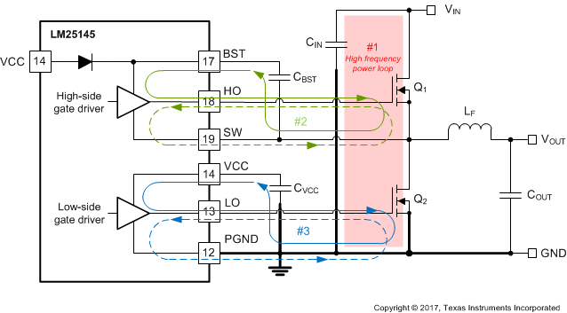
Proper PCB design and layout is important in a high current, fast switching circuit (with high current and voltage slew rates) to assure appropriate device operation and design robustness. As expected, certain issues must be considered before designing a PCB layout using the LM25145. The high-frequency power loop of the buck converter power stage is denoted by #1 in the shaded area of Figure 75. The topological architecture of a buck converter means that particularly high di/dt current flows in the components of loop #1, and it becomes mandatory to reduce the parasitic inductance of this loop by minimizing its effective loop area. Also important are the gate drive loops of the low-side and high-side MOSFETs, denoted by #2 and #3, respectively, in Figure 75.
 Figure 75. DC-DC Regulator Ground System With Power Stage and Gate Drive Circuit Switching Loops
11.1.1 Power Stage Layout
- Input capacitors, output capacitors, and MOSFETs are the constituent components in the power stage of a buck regulator and are typically placed on the top side of the PCB (solder side). The benefits of convective heat transfer are maximized because of leveraging any system-level airflow. In a two-sided PCB layout, small-signal components are typically placed on the bottom side (component side). At least one inner plane should be inserted, connected to ground, to shield and isolate the small-signal traces from noisy power traces and lines.
- The DC-DC converter has several high-current loops. Minimize the area of these loops in order to suppress generated switching noise and parasitic loop inductance and optimize switching performance.
- Loop #1: The most important loop to minimize the area of is the path from the input capacitor(s) through the high- and low-side MOSFETs, and back to the capacitor(s) through the ground connection. Connect the input capacitor(s) negative terminal close to the source of the low-side MOSFET (at ground). Similarly, connect the input capacitor(s) positive terminal close to the drain of the high-side MOSFET (at VIN). Refer to loop #1 of Figure 75.
- Another loop, not as critical though as loop #1, is the path from the low-side MOSFET through the inductor and output capacitor(s), and back to source of the low-side MOSFET through ground. Connect the source of the low-side MOSFET and negative terminal of the output capacitor(s) at ground as close as possible.
- The PCB trace defined as SW node, which connects to the source of the high-side (control) MOSFET, the drain of the low-side (synchronous) MOSFET and the high-voltage side of the inductor, should be short and wide. However, the SW connection is a source of injected EMI and thus should not be too large.
- Follow any layout considerations of the MOSFETs as recommended by the MOSFET manufacturer, including pad geometry and solder paste stencil design.
- The SW pin connects to the switch node of the power conversion stage, and it acts as the return path for the high-side gate driver. The parasitic inductance inherent to loop #1 in Figure 75 and the output capacitance (COSS) of both power MOSFETs form a resonant circuit that induces high frequency (>100 MHz) ringing on the SW node. The voltage peak of this ringing, if not controlled, can be significantly higher than the input voltage. Ensure that the peak ringing amplitude does not exceed the absolute maximum rating limit for the SW pin. In many cases, a series resistor and capacitor snubber network connected from the SW node to GND damps the ringing and decreases the peak amplitude. Provide provisions for snubber network components in the PCB layout. If testing reveals that the ringing amplitude at the SW pin is excessive, then include snubber components as needed.
11.1.2 Gate Drive Layout
The LM25145 high-side and low-side gate drivers incorporate short propagation delays, adaptive dead-time control and low-impedance output stages capable of delivering large peak currents with very fast rise and fall times to facilitate rapid turnon and turnoff transitions of the power MOSFETs. Very high di/dt can cause unacceptable ringing if the trace lengths and impedances are not well controlled.
Minimization of stray or parasitic gate loop inductance is key to optimizing gate drive switching performance, whether it be series gate inductance that resonates with MOSFET gate capacitance or common source inductance (common to gate and power loops) that provides a negative feedback component opposing the gate drive command, thereby increasing MOSFET switching times. The following loops are important:
- Loop #2: high-side MOSFET, Q1. During the high-side MOSFET turn on, high current flows from the boot capacitor through the gate driver and high-side MOSFET, and back to the negative terminal of the boot capacitor through the SW connection. Conversely, to turn off the high-side MOSFET, high current flows from the gate of the high-side MOSFET through the gate driver and SW, and back to the source of the high-side MOSFET through the SW trace. Refer to loop #2 of Figure 75.
- Loop #3: low-side MOSFET, Q2. During the low-side MOSFET turnon, high current flows from the VCC decoupling capacitor through the gate driver and low-side MOSFET, and back to the negative terminal of the capacitor through ground. Conversely, to turn off the low-side MOSFET, high current flows from the gate of the low-side MOSFET through the gate driver and GND, and back to the source of the low-side MOSFET through ground. Refer to loop #3 of Figure 75.
The following circuit layout guidelines are strongly recommended when designing with high-speed MOSFET gate drive circuits.
- Connections from gate driver outputs, HO and LO, to the respective gate of the high-side or low-side MOSFET should be as short as possible to reduce series parasitic inductance. Use 0.65 mm (25 mils) or wider traces. Use via(s), if necessary, of at least 0.5 mm (20 mils) diameter along these traces. Route HO and SW gate traces as a differential pair from the LM25145 to the high-side MOSFET, taking advantage of flux cancellation.
- Minimize the current loop path from the VCC and BST pins through their respective capacitors as these provide the high instantaneous current, up to 3.5 A, to charge the MOSFET gate capacitances. Specifically, locate the bootstrap capacitor, CBST, close to the BST and SW pins of the LM25145 to minimize the area of loop #2 associated with the high-side driver. Similarly, locate the VCC capacitor, CVCC, close to the VCC and PGND pins of the LM25145 to minimize the area of loop #3 associated with the low-side driver.
- Placing a 2-Ω to 10-Ω resistor in series with the BST capacitor slows down the high-side MOSFET turnon transition, serving to reduce the voltage ringing and peak amplitude at the SW node at the expense of increased MOSFET turnon power loss.
11.1.3 PWM Controller Layout
With the proviso to locate the controller as close as possible to the MOSFETs to minimize gate driver trace runs, the components related to the analog and feedback signals, current limit setting and temperature sense are considered in the following:
- Separate power and signal traces, and use a ground plane to provide noise shielding.
- Place all sensitive analog traces and components such as COMP, FB, RT, ILIM and SS/TRK away from high-voltage switching nodes such as SW, HO, LO or BST to avoid mutual coupling. Use internal layer(s) as ground plane(s). Pay particular attention to shielding the feedback (FB) trace from power traces and components.
- The upper feedback resistor can be connected directly to the output voltage sense point at the load device or the bulk capacitor at the converter side.
- Connect the ILIM setting resistor from the drain of the low-side MOSFET to ILIM and make the connections as close as possible to the LM25145. The trace from the ILIM pin to the resistor should avoid coupling to a high-voltage switching net.
- Minimize the loop area from the VCC and VIN pins through their respective decoupling capacitors to the GND pin. Locate these capacitors as close as possible to the LM25145.
11.1.4 Thermal Design and Layout
The useful operating temperature range of a PWM controller with integrated gate drivers and bias supply LDO regulator is greatly affected by:
- average gate drive current requirements of the power MOSFETs;
- switching frequency;
- operating input voltage (affecting bias regulator LDO voltage drop and hence its power dissipation);
- thermal characteristics of the package and operating environment.
For a PWM controller to be useful over a particular temperature range, the package must allow for the efficient removal of the heat produced while keeping the junction temperature within rated limits. The LM25145 controller is available in a small 3.5-mm × 4.5-mm 20-pin VQFN (RGY) PowerPAD™ package to cover a range of application requirements. The thermal metrics of this package are summarized in Thermal Information. The application report IC Package Thermal Metrics (SPRA953) provides detailed information regarding the thermal information table.
The 20-pin VQFN package offers a means of removing heat from the semiconductor die through the exposed thermal pad at the base of the package. While the exposed pad of the package is not directly connected to any leads of the package, it is thermally connected to the substrate of the LM25145 device (ground). This allows a significant improvement in heat sinking, and it becomes imperative that the PCB is designed with thermal lands, thermal vias, and a ground plane to complete the heat removal subsystem. The exposed pad of the LM25145 is soldered to the ground-connected copper land on the PCB directly underneath the device package, reducing the thermal resistance to a very low value. Wide traces of the copper tying in the no-connect pins of the LM25145 (pins 9 and 16) and connection to this thermal land helps to dissipate heat.
Numerous vias with a 0.3-mm diameter connected from the thermal land to the internal and solder-side ground plane(s) are vital to help dissipation. In a multi-layer PCB design, a solid ground plane is typically placed on the PCB layer below the power components. Not only does this provide a plane for the power stage currents to flow but it also represents a thermally conductive path away from the heat generating devices.
The thermal characteristics of the MOSFETs also are significant. The drain pad of the high-side MOSFET is normally connected to a VIN plane for heat sinking. The drain pad of the low-side MOSFET is tied to the SW plane, but the SW plane area is purposely kept relatively small to mitigate EMI concerns.
11.1.5 Ground Plane Design
As mentioned previously, using one or more of the inner PCB layers as a solid ground plane is recommended. A ground plane offers shielding for sensitive circuits and traces and also provides a quiet reference potential for the control circuitry. Connect the PGND pin to the system ground plane using an array of vias under the exposed pad. Also connect the PGND directly to the return terminals of the input and output capacitors. The PGND net contains noise at the switching frequency and can bounce because of load current variations. The power traces for PGND, VIN and SW can be restricted to one side of the ground plane. The other side of the ground plane contains much less noise and is ideal for sensitive analog trace routes.
11.2 Layout Example
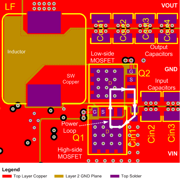
Figure 76 shows an example PCB layout based on the LM5145EVM-HD-20A 20-A design. The power component connections are made on the top layer with wide, copper-filled areas. A power ground plane is placed on layer 2 with 6 mil (0.15 mm) spacing to the top layer. The small area of buck regulator hot loop is denoted by the white border in Figure 76.
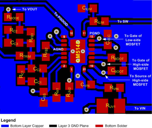
The LM25145 is located on the bottom side with a surrounding analog ground plane for sensitive analog components as shown in Figure 77. The analog ground plane (AGND) and power ground plane (PGND) are connected at a single point directly under the IC (at the die attach pad or DAP). Refer to the LM5145 EVM User's Guide (SNVU545) for more detail.
 Figure 76. LM25145 Power Stage PCB Layout
 Figure 77. LM25145 Controller PCB Layout (Viewed From Top)