ZHCSGD0 June 2017 LM25145
PRODUCTION DATA.
- 1 特性
- 2 应用
- 3 说明
- 4 修订历史记录
- 5 说明 (续)
- 6 Pin Configuration and Functions
- 7 Specifications
-
8 Detailed Description
- 8.1 Overview
- 8.2 Functional Block Diagram
- 8.3
Feature Description
- 8.3.1 Input Range (VIN)
- 8.3.2 Output Voltage Setpoint and Accuracy (FB)
- 8.3.3 High-Voltage Bias Supply Regulator (VCC)
- 8.3.4 Precision Enable (EN/UVLO)
- 8.3.5 Power Good Monitor (PGOOD)
- 8.3.6 Switching Frequency (RT, SYNCIN)
- 8.3.7 Configurable Soft-Start (SS/TRK)
- 8.3.8 Voltage-Mode Control (COMP)
- 8.3.9 Gate Drivers (LO, HO)
- 8.3.10 Current Sensing and Overcurrent Protection (ILIM)
- 8.3.11 OCP Duty Cycle Limiter
- 8.4 Device Functional Modes
-
9 Application and Implementation
- 9.1 Application Information
- 9.2 Typical Applications
- 10Power Supply Recommendations
- 11Layout
- 12器件和文档支持
- 13机械、封装和可订购信息
7 Specifications
7.1 Absolute Maximum Ratings
Over the recommended operating junction temperature range of –40°C to 125°C (unless otherwise noted).(1)| MIN | MAX | UNIT | ||
|---|---|---|---|---|
| Input voltages | VIN | –0.3 | 45 | V |
| SW | –1 | 45 | ||
| SW (20-ns transient) | –5 | 45 | ||
| ILIM | –1 | 45 | ||
| EN/UVLO | –0.3 | 45 | ||
| VCC | –0.3 | 14 | ||
| FB, COMP, SS/TRK, RT | –0.3 | 6 | ||
| SYNCIN | –0.3 | 14 | ||
| Output voltages | BST | –0.3 | 60 | V |
| BST to VCC | 45 | |||
| BST to SW | –0.3 | 14 | ||
| VCC to BST (20-ns transient) | 7 | |||
| LO (20-ns transient) | –3 | |||
| PGOOD | –0.3 | 14 | ||
| Operating junction temperature, TJ | 150 | °C | ||
| Storage temperature, Tstg | –55 | 150 | °C | |
(1) Stresses beyond those listed under Absolute Maximum Ratings may cause permanent damage to the device. These are stress ratings only, which do not imply functional operation of the device at these or any other conditions beyond those indicated under Recommended Operating Conditions. Exposure to absolute-maximum-rated conditions for extended periods may affect device reliability.
7.2 ESD Ratings
| VALUE | UNIT | |||
|---|---|---|---|---|
| V(ESD) | Electrostatic discharge | Human-body model (HBM), per ANSI/ESDA/JEDEC JS-001(1) | ±2000 | V |
| Charged-device model (CDM), per JEDEC specification JESD22-C101(2) | ±1000 | |||
(1) JEDEC document JEP155 states that 500-V HBM allows safe manufacturing with a standard ESD control process.
(2) JEDEC document JEP157 states that 250-V CDM allows safe manufacturing with a standard ESD control process.
7.3 Recommended Operating Conditions
Over the recommended operating junction temperature range of –40°C to 125°C (unless otherwise noted).(1)| MIN | NOM | MAX | UNIT | |||
|---|---|---|---|---|---|---|
| VI | Input voltages | VIN | 6 | 42 | V | |
| SW | –1 | 42 | ||||
| ILIM | –1 | 42 | ||||
| External VCC bias rail | 8 | 13 | ||||
| EN/UVLO | 0 | 42 | ||||
| VO | Output voltages | BST | –0.3 | 55 | V | |
| BST to VCC | 42 | |||||
| BST to SW | 5 | 13 | ||||
| PGOOD | 13 | |||||
| ISINK, ISRC | Sink/source currents | SYNCOUT | –1 | 1 | mA | |
| PGOOD | 2 | |||||
| TJ | Operating junction temperature | –40 | 125 | °C | ||
(1) Recommended Operating Conditions are conditions under which the device is intended to be functional. For specifications and test conditions, see Electrical Characteristics.
7.4 Thermal Information
| THERMAL METRIC(1) | LM25145 | UNIT | |
|---|---|---|---|
| RGY (VQFN) | |||
| 20 PINS | |||
| RθJA | Junction-to-ambient thermal resistance | 36.8 | °C/W |
| RθJC(top) | Junction-to-case (top) thermal resistance | 28 | °C/W |
| RθJB | Junction-to-board thermal resistance | 11.8 | °C/W |
| ψJT | Junction-to-top characterization parameter | 0.4 | °C/W |
| ψJB | Junction-to-board characterization parameter | 11.7 | °C/W |
| RθJC(bot) | Junction-to-case (bottom) thermal resistance | 2.1 | °C/W |
(1) For more information about traditional and new thermal metrics, see the Semiconductor and IC Package Thermal Metrics application report.
7.5 Electrical Characteristics
Typical values correspond to TJ = 25°C. Minimum and maximum limits apply over the –40°C to 125°C junction temperature range unless otherwise stated. VIN = 24 V, VEN/UVLO = 1.5 V, RRT = 25 kΩ unless otherwise stated.(1)(2)| PARAMETER | TEST CONDITIONS | MIN | TYP | MAX | UNIT | |
|---|---|---|---|---|---|---|
| INPUT SUPPLY | ||||||
| VIN | Operating input voltage range | 6 | 42 | V | ||
| IQ-RUN | Operating input current, not switching | VEN/UVLO = 1.5 V, VSS/TRK = 0 V | 1.8 | 2.1 | mA | |
| IQ-STBY | Standby input current | VEN/UVLO = 1 V | 1.75 | 2 | mA | |
| IQ-SDN | Shutdown input current | VEN/UVLO = 0 V, VVCC < 1 V | 13.5 | 16 | µA | |
| VCC REGULATOR | ||||||
| VVCC | VCC regulation voltage | VSS/TRK = 0 V, 9 V ≤ VVIN ≤ 42 V, 0 mA < IVCC ≤ 20 mA |
7.3 | 7.5 | 7.7 | V |
| VVCC-LDO | VIN to VCC dropout voltage | VVIN = 6 V, VSS/TRK = 0 V, IVCC = 20 mA | 0.25 | 0.63 | V | |
| ISC-LDO | VCC short-circuit current | VSS/TRK = 0 V, VVCC = 0 V | 40 | 50 | 70 | mA |
| VVCC-UV | VCC undervoltage threshold | VVCC rising | 4.8 | 4.93 | 5.2 | V |
| VVCC-UVH | VCC undervoltage hysteresis | Rising threshold – falling threshold | 0.26 | V | ||
| VVCC-EXT | Minimum external bias supply voltage | Voltage required to disable VCC regulator | 8 | V | ||
| IVCC | External VCC input current, not switching | VSS/TRK = 0 V, VVCC = 13 V | 2.1 | mA | ||
| ENABLE AND INPUT UVLO | ||||||
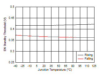
| VSDN | Shutdown to standby threshold | VEN/UVLO rising | 0.42 | V | ||
| VSDN-HYS | Shutdown threshold hysteresis | EN/UVLO rising – falling threshold | 50 | mV | ||
| VEN | Standby to operating threshold | VEN/UVLO rising | 1.164 | 1.2 | 1.236 | V |
| IEN-HYS | Standby to operating hysteresis current | VEN/UVLO = 1.5 V | 9 | 10 | 11 | µA |
| ERROR AMPLIFIER | ||||||
| VREF | FB reference voltage | FB connected to COMP | 792 | 800 | 808 | mV |
| IFB-BIAS | FB input bias current | VFB = 0.8 V | –0.1 | 0.1 | µA | |
| VCOMP-OH | COMP output high voltage | VFB = 0 V, COMP sourcing 1 mA | 5 | V | ||
| VCOMP-OL | COMP output low voltage | COMP sinking 1 mA | 0.3 | V | ||
| AVOL | DC gain | 94 | dB | |||
| GBW | Unity gain bandwidth | 6.5 | MHz | |||
| SOFT-START AND VOLTAGE TRACKING | ||||||
| ISS | SS/TRK capacitor charging current | VSS/TRK = 0 V | 8.5 | 10 | 12 | µA |
| RSS | SS/TRK discharge FET resistance | VEN/UVLO = 1 V, VSS/TRK = 0.1 V | 11 | Ω | ||
| VSS-FB | SS/TRK to FB offset | –15 | 15 | mV | ||
| VSS-CLAMP | SS/TRK clamp voltage | VSS/TRK – VFB, VFB = 0.8 V | 115 | mV | ||
| POWER GOOD INDICATOR | ||||||
| PGUTH | FB upper threshold for PGOOD high to low | % of VREF, VFB rising | 106% | 108% | 110% | |
| PGLTH | FB lower threshold for PGOOD high to low | % of VREF, VFB falling | 90% | 92% | 94% | |
| PGHYS_U | PGOOD upper threshold hysteresis | % of VREF | 3% | |||
| PGHYS_L | PGOOD lower threshold hysteresis | % of VREF | 2% | |||
| TPG-RISE | PGOOD rising filter | FB to PGOOD rising edge | 25 | µs | ||
| TPG-FALL | PGOOD falling filter | FB to PGOOD falling edge | 25 | µs | ||
| VPG-OL | PGOOD low state output voltage | VFB = 0.9 V, IPGOOD = 2 mA | 150 | mV | ||
| IPG-OH | PGOOD high state leakage current | VFB = 0.8 V, VPGOOD = 13 V | 100 | nA | ||
| OSCILLATOR | ||||||
| FSW1 | Oscillator Frequency – 1 | RRT = 100 kΩ | 100 | kHz | ||
| FSW2 | Oscillator Frequency – 2 | RRT = 25 kΩ | 380 | 400 | 420 | kHz |
| FSW3 | Oscillator Frequency – 3 | RRT = 12.5 kΩ | 780 | kHz | ||
| SYNCHRONIZATION INPUT AND OUTPUT | ||||||
| FSYNC | SYNCIN external clock frequency range | % of nominal frequency set by RRT | –20% | +50% | ||
| VSYNC-IH | Minimum SYNCIN input logic high | 2 | V | |||
| VSYNC-IL | Maximum SYNCIN input logic low | 0.8 | V | |||
| RSYNCIN | SYNCIN input resistance | VSYNCIN = 3 V | 20 | kΩ | ||
| TSYNCI-PW | SYNCIN input minimum pulsewidth | Minimum high state or low state duration | 50 | ns | ||
| VSYNCO-OH | SYNCOUT high state output voltage | ISYNCOUT = –1 mA (sourcing) | 3 | V | ||
| VSYNCO-OL | SYNCOUT low state output voltage | ISYNCOUT = 1 mA (sinking) | 0.4 | V | ||
| TSYNCOUT | Delay from HO rising to SYNCOUT leading edge | VSYNCIN = 0 V, TS = 1/FSW, FSW set by RRT |
TS/2 – 140 | ns | ||
| TSYNCIN | Delay from SYNCIN leading edge to HO rising | 50% to 50% | 150 | ns | ||
| BOOTSTRAP DIODE AND UNDERVOLTAGE THRESHOLD | ||||||
| VBST-FWD | Diode forward voltage, VCC to BST | VCC to BST, BST pin sourcing 20 mA | 0.75 | 0.9 | V | |
| IQ-BST | BST to SW quiescent current, not switching | VSS/TRK = 0 V, VSW = 24 V, VBST = 30 V | 80 | µA | ||
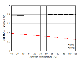
| VBST-UV | BST to SW undervoltage detection | VBST – VSW falling | 3.4 | V | ||
| VBST-HYS | BST to SW undervoltage hysteresis | VBST – VSW rising | 0.42 | V | ||
| PWM CONTROL | ||||||
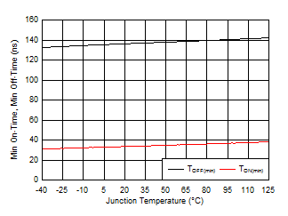
| TON(MIN) | Minimum controllable on-time | VBST – VSW = 7 V, HO 50% to 50% | 40 | 60 | ns | |
| TOFF(MIN) | Minimum off-time | VBST – VSW = 7 V, HO 50% to 50% | 140 | 200 | ns | |
| DC100kHz | Maximum duty cycle | FSW = 100 kHz, 6 V ≤ VVIN ≤ 42 V | 98% | 99% | ||
| DC400kHz | FSW = 400 kHz, 6 V ≤ VVIN ≤ 42 V | 90% | 94% | |||
| VRAMP(min) | Ramp valley voltage (COMP at 0% duty cycle) | 300 | mV | |||
| kFF | PWM feedforward gain (VIN / VRAMP) | 6 V ≤ VVIN ≤ 42 V | 15 | V/V | ||
| OVERCURRENT PROTECT (OCP) – VALLEY CURRENT LIMITING | ||||||
| IRS | ILIM source current, RSENSE mode | Low voltage detected at ILIM | 90 | 100 | 110 | µA |
| IRDSON | ILIM source current, RDS(on) mode | SW voltage detected at ILIM, TJ = 25°C | 180 | 200 | 220 | µA |
| IRSTC | ILIM current tempco | RDS-ON mode | 4500 | ppm/°C | ||
| IRDSONTC | ILIM current tempco | RSENSE mode | 0 | ppm/°C | ||
| VILIM-TH | ILIM comparator threshold at ILIM | –8 | –2 | 3.5 | mV | |
| SHORT-CIRCUIT PROTECT (SCP) – DUTY CYCLE CLAMP | ||||||
| VCLAMP-OS | Clamp offset voltage – no current limiting | CLAMP to COMP steady state offset voltage | 0.2 + VVIN/75 | V | ||
| VCLAMP-MIN | Minimum clamp voltage | CLAMP voltage with continuous current limiting | 0.3 + VVIN/150 | V | ||
| HICCUP MODE FAULT PROTECTION | ||||||
| CHICC-DEL | Hiccup mode activation delay | Clock cycles with current limiting before hiccup off-time activated | 128 | cycles | ||
| CHICCUP | Hiccup mode off-time after activation | Clock cycles with no switching followed by SS/TRK release | 8192 | cycles | ||
| DIODE EMULATION | ||||||
| VZCD-SS | Zero-cross detect (ZCD) soft-start ramp | ZCD threshold measured at SW pin 50 clock cycles after first HO pulse |
0 | mV | ||
| VZCD-DIS | Zero-cross detect disable threshold (CCM) | ZCD threshold measured at SW pin 1000 clock cycles after first HO pulse |
200 | mV | ||
| VDEM-TH | Diode emulation zero-cross threshold | Measured at SW with VSW rising | –5 | 0 | 5 | mV |
| GATE DRIVERS | ||||||
| RHO-UP | HO high-state resistance, HO to BST | VBST – VSW = 7 V, IHO = –100 mA | 1.5 | Ω | ||
| RHO-DOWN | HO low-state resistance, HO to SW | VBST – VSW = 7 V, IHO = 100 mA | 0.9 | Ω | ||
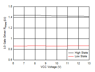
| RLO-UP | LO high-state resistance, LO to VCC | VBST – VSW = 7 V, ILO = –100 mA | 1.5 | Ω | ||
| RLO-DOWN | LO low-state resistance, LO to PGND | VBST – VSW = 7 V, ILO = 100 mA | 0.9 | Ω | ||
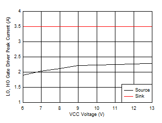
| IHOH, ILOH | HO, LO source current | VBST – VSW = 7 V, HO = SW, LO = AGND | 2.3 | A | ||
| IHOL, ILOL | HO, LO sink current | VBST – VSW = 7 V, HO = BST, LO = VCC | 3.5 | A | ||
| THERMAL SHUTDOWN | ||||||
| TSD | Thermal shutdown threshold | TJ rising | 175 | °C | ||
| TSD-HYS | Thermal shutdown hysteresis | 20 | °C | |||
(1) All minimum and maximum limits are specified by correlating the electrical characteristics to process and temperature variations and applying statistical process control.
(2) The junction temperature (TJ in °C) is calculated from the ambient temperature (TA in °C) and power dissipation (PD in Watts) as follows: TJ = TA + (PD • RθJA) where RθJA (in °C/W) is the package thermal impedance provided in Thermal Information.
7.6 Switching Characteristics
Over operating free-air temperature range (unless otherwise noted).| PARAMETER | TEST CONDITIONS | MIN | TYP | MAX | UNIT | |
|---|---|---|---|---|---|---|
| THO-TR
TLO-TR |
HO, LO rise times | VBST – VSW = 7 V, CLOAD = 1 nF, 20% to 80% | 7 | ns | ||
| THO-TF
TLO-TF |
HO, LO fall times | VBST – VSW = 7 V, CLOAD = 1 nF, 80% to 20% | 4 | ns | ||
| THO-DT | HO turnon dead time | VBST – VSW = 7 V, LO off to HO on, 50% to 50% | 14 | ns | ||
| TLO-DT | LO turnon dead time | VBST – VSW = 7 V, HO off to LO on, 50% to 50% | 14 | ns | ||
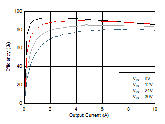
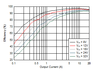
7.7 Typical Characteristics
VVIN = 24 V, RRT = 25 kΩ, SYNCIN tied to VCC, EN/UVLO tied to VIN (unless otherwise noted).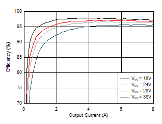
| VOUT = 12 V See Figure 57 |
VSYNCIN = VVCC | FSW = 425 kHz RRT = 23.7 kΩ |
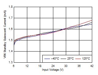
| VSW = 0 V | VEN/UVLO = 1 V |
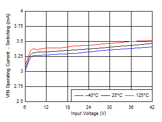
| VSW = 0 V | HO, LO Open |

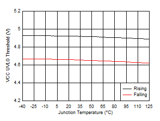
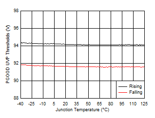
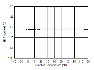

| VSW = 0 V |
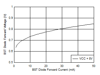


| VSS/TRK = 0 V |
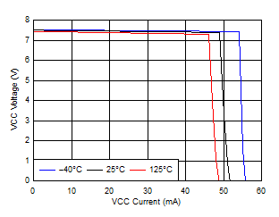
| VIN = 12 V |

| VOUT = 12 V See Figure 57 |
VSYNCIN = 0 V | FSW = 425 kHz RRT = 23.7 kΩ |
(VOUT Supplies Bias Power to VCC)
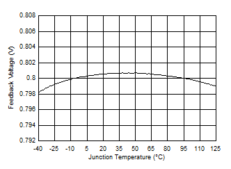
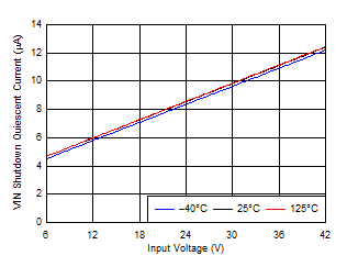
| VSW = 0 V | VEN/UVLO = 0 V |
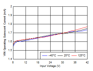
| VSW = 0 V | VEN/UVLO = VVIN | VSS/TRK = 0 V |
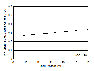
| VSW = 0 V | VVCC = VBST = VILIM | VFB = 0 V |
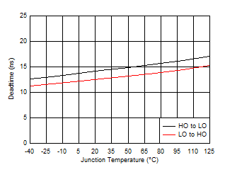
| VSW = 0 V |



| VIN = 6 V |


