ZHCSGD0 June 2017 LM25145
PRODUCTION DATA.
- 1 特性
- 2 应用
- 3 说明
- 4 修订历史记录
- 5 说明 (续)
- 6 Pin Configuration and Functions
- 7 Specifications
-
8 Detailed Description
- 8.1 Overview
- 8.2 Functional Block Diagram
- 8.3
Feature Description
- 8.3.1 Input Range (VIN)
- 8.3.2 Output Voltage Setpoint and Accuracy (FB)
- 8.3.3 High-Voltage Bias Supply Regulator (VCC)
- 8.3.4 Precision Enable (EN/UVLO)
- 8.3.5 Power Good Monitor (PGOOD)
- 8.3.6 Switching Frequency (RT, SYNCIN)
- 8.3.7 Configurable Soft-Start (SS/TRK)
- 8.3.8 Voltage-Mode Control (COMP)
- 8.3.9 Gate Drivers (LO, HO)
- 8.3.10 Current Sensing and Overcurrent Protection (ILIM)
- 8.3.11 OCP Duty Cycle Limiter
- 8.4 Device Functional Modes
-
9 Application and Implementation
- 9.1 Application Information
- 9.2 Typical Applications
- 10Power Supply Recommendations
- 11Layout
- 12器件和文档支持
- 13机械、封装和可订购信息
8 Detailed Description
8.1 Overview
The LM25145 is a 42-V synchronous buck controller that features all of the functions necessary to implement a high efficiency step-down power supply with output voltage ranging from 0.8 V to 40 V. The voltage-mode control architecture uses input feedforward for excellent line transient response over a wide VIN range. Voltage-mode control supports the wide duty cycle range for high input voltage and low dropout applications as well as when a high voltage conversion ratio (for example, 10-to-1) is required. Current sensing for cycle-by-cycle current limit can be implemented with either the low-side FET RDS(on) or a current sense resistor. The operating frequency is programmable from 100 kHz to 1 MHz. The LM25145 drives external high-side and low-side NMOS power switches with robust 7.5-V gate drivers suitable for standard threshold MOSFETs. Adaptive dead-time control between the high-side and low-side drivers is designed to minimize body diode conduction during switching transitions. An external bias supply can be connected to the VCC pin to improve efficiency in high-voltage applications. A user-selectable diode emulation feature enables discontinuous conduction mode operation for improved efficiency and lower dissipation at light-load conditions.
8.2 Functional Block Diagram

8.3 Feature Description
8.3.1 Input Range (VIN)
The LM25145 operational input voltage range is from 6 V to 42 V. The device is intended for step-down conversions from 12-V, 24-V, 28-V and 36-V unregulated, semiregulated, and fully-regulated supply rails. The application circuit of Figure 31 shows all the necessary components to implement an LM25145-based wide-VIN step-down regulator using a single supply. The LM25145 uses an internal LDO subregulator to provide a 7.5-V VCC bias rail for the gate drive and control circuits (assuming the input voltage is higher than 7.5 V plus the necessary subregulator dropout specification).
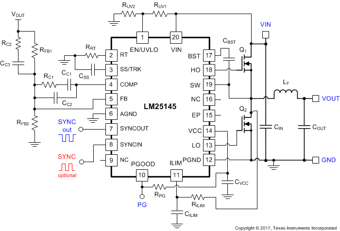 Figure 31. Schematic Diagram for VIN Operating Range of 6 V to 42 V
In high voltage applications, take extra care to ensure the VIN pin does not exceed the absolute maximum voltage rating of 55 V during line or load transient events. Voltage ringing on the VIN pin that exceeds the Absolute Maximum Ratings can damage the IC. Use high-quality ceramic input capacitors to minimize ringing. An RC filter from the input rail to the VIN pin (for example, 4.7 Ω and 0.1 µF) provides supplementary filtering at the VIN pin.
8.3.2 Output Voltage Setpoint and Accuracy (FB)
The reference voltage at the FB pin is set at 0.8 V with a feedback system accuracy over the full junction temperature range of ±1%. Junction temperature range for the device is –40°C to +125°C. While dependent on switching frequency and load current levels, the LM25145 is generally capable of providing output voltages in the range of 0.8 V to a maximum of slightly less than VIN. The DC output voltage setpoint during normal operation is set by the feedback resistor network, RFB1 and RFB2, connected to the output.
8.3.3 High-Voltage Bias Supply Regulator (VCC)
The LM25145 contains an internal high-voltage VCC regulator that provides a bias supply for the PWM controller and its gate drivers for the external MOSFETs. The input pin (VIN) can be connected directly to an input voltage source up to 42 V. The output of the VCC regulator is set to 7.5 V. However, when the input voltage is below the VCC setpoint level, the VCC output tracks VIN with a small voltage drop. Connect a ceramic decoupling capacitor between 1 µF and 5 µF from VCC to AGND for stability.
The VCC regulator output has a current limit of 40 mA (minimum). At power up, the regulator sources current into the capacitor connected to the VCC pin. When the VCC voltage exceeds its rising UVLO threshold of 4.93 V, the output is enabled (if EN/UVLO is above 1.2 V) and the soft-start sequence begins. The output remain active until the VCC voltage falls below its falling UVLO threshold of 4.67 V (typical) or if EN/UVLO goes to a standby or shutdown state.
Internal power dissipation of the VCC regulator can be minimized by connecting the output voltage or an auxiliary bias supply rail (up to 13 V) to VCC using a diode DVCC as shown in Figure 32. A diode in series with the input prevents reverse current flow from VCC to VIN if the input voltage falls below the external VCC rail.
 Figure 32. VCC Bias Supply Connection From VOUT or Auxiliary Supply
Note that a finite bias supply regulator dropout voltage exists and is manifested to a larger extent when driving high gate charge (QG) power MOSFETs at elevated switching frequencies. For example, at VVIN = 6 V, the VCC voltage is 5.8 V with a DC operating current, IVCC, of 20 mA. Such a low gate drive voltage may be insufficient to fully enhance the power MOSFETs. At the very least, MOSFET on-state resistance, RDS(ON), may increase at such low gate drive voltage.
Here are the main considerations when operating at input voltages below 7.5 V:
- Increased MOSFET RDS(on) at lower VGS, leading to Increased conduction losses and reduced OCP setpoint.
- Increased switching losses given the slower switching times when operating at lower gate voltages.
- Restricted range of suitable power MOSFETs to choose from (MOSFETs with RDS(on) rated at VGS = 4.5 V become mandatory).
8.3.4 Precision Enable (EN/UVLO)
The EN/UVLO input supports adjustable input undervoltage lockout (UVLO) with hysteresis programmed by the resistor values for application specific power-up and power-down requirements. EN/UVLO connects to a comparator-based input referenced to a 1.2-V bandgap voltage. An external logic signal can be used to drive the EN/UVLO input to toggle the output ON and OFF and for system sequencing or protection. The simplest way to enable the operation of the LM25145 is to connect EN/UVLO directly to VIN. This allows self start-up of the LM25145 when VCC is within its valid operating range. However, many applications benefit from using a resistor divider RUV1 and RUV2 as shown in Figure 33 to establish a precision UVLO level.
Use Equation 1 and Equation 2 to calculate the UVLO resistors given the required input turnon and turnoff voltages.


 Figure 33. Programmable Input Voltage UVLO Turnon and Turnoff
The LM25145 enters a low IQ shutdown mode when EN/UVLO is pulled below approximately 0.4 V. The internal LDO regulator powers off and the internal bias supply rail collapses, shutting down the bias currents of the LM25145. The LM25145 operates in standby mode when the EN/UVLO voltage is between the hard shutdown and precision enable (standby) thresholds.
8.3.5 Power Good Monitor (PGOOD)
The LM25145 provides a PGOOD flag pin to indicate when the output voltage is within a regulation window. Use the PGOOD signal as shown in Figure 34 for start-up sequencing of downstream converters, fault protection, and output monitoring. PGOOD is an open-drain output that requires a pullup resistor to a DC supply not greater than 13 V. The typical range of pullup resistance is 10 kΩ to 100 kΩ. If necessary, use a resistor divider to decrease the voltage from a higher voltage pullup rail.
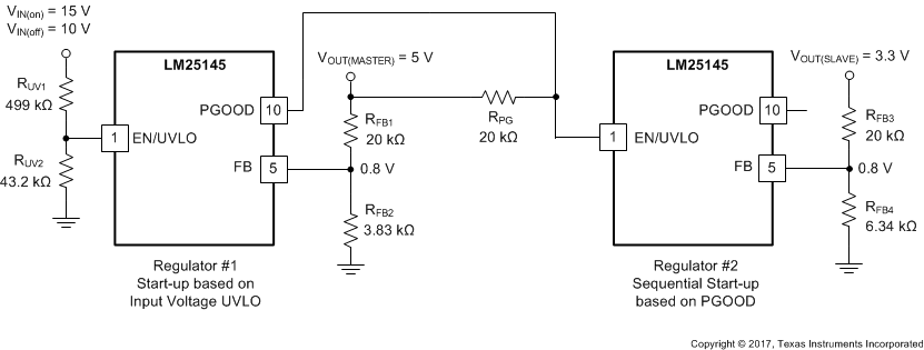 Figure 34. Master-Slave Sequencing Implementation Using PGOOD and EN/UVLO
When the FB voltage exceeds 94% of the internal reference VREF, the internal PGOOD switch turns off and PGOOD can be pulled high by the external pullup. If the FB voltage falls below 92% of VREF, the internal PGOOD switch turns on, and PGOOD is pulled low to indicate that the output voltage is out of regulation. Similarly, when the FB voltage exceeds 108% of VREF, the internal PGOOD switch turns on, pulling PGOOD low. If the FB voltage subsequently falls below 105% of VREF, the PGOOD switch is turned off and PGOOD is pulled high. PGOOD has a built-in deglitch delay of 25 µs.
8.3.6 Switching Frequency (RT, SYNCIN)
There are two options for setting the switching frequency, FSW, of the LM25145, thus providing a power supply designer with a level of flexibility when choosing external components for various applications. To adjust the frequency, use a resistor from the RT pin to AGND, or synchronize the LM25145 to an external clock signal through the SYNCIN pin.
8.3.6.1 Frequency Adjust
Adjust the LM25145 free-running switching frequency by using a resistor from the RT pin to AGND. The switching frequency range is from 100 kHz to 1 MHz. The frequency set resistance, RRT, is governed by Equation 3. E96 standard-value resistors for common switching frequencies are given in Table 1.

Table 1. Frequency Set Resistors
| SWITCHING FREQUENCY (kHz) | FREQUENCY SET RESISTANCE (kΩ) |
|---|---|
| 100 | 100 |
| 200 | 49.9 |
| 250 | 40.2 |
| 300 | 33.2 |
| 400 | 24.9 |
| 500 | 20 |
| 750 | 13.3 |
| 1000 | 10 |
8.3.6.2 Clock Synchronization
Apply an external clock synchronization signal to the LM25145 to synchronize switching in both frequency and phase. Requirements for the external clock SYNC signal are:
- Clock frequency range: 100 kHz to 1 MHz
- Clock frequency: –20% to +50% of the free-running frequency set by RRT
- Clock maximum voltage amplitude: 13 V
- Clock minimum pulse width: 50 ns
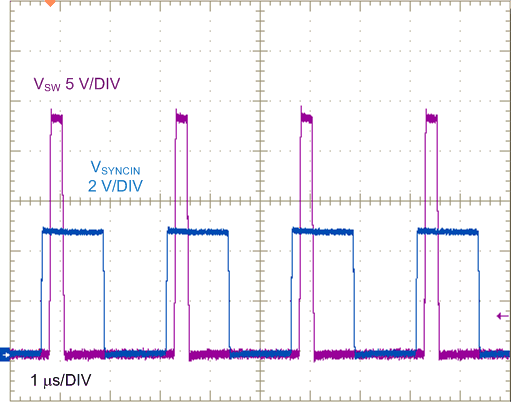 Figure 35. Typical 400-kHz SYNCIN and SW Voltage Waveforms
Figure 35 shows a clock signal at 400 kHz and the corresponding SW node waveform (VIN = 24 V, VOUT = 5 V, free-running frequency = 280 kHz). The SW voltage waveform is synchronized with respect to the rising edge of SYNCIN. The rising edge of the SW voltage is phase delayed relative to SYNCIN by approximately 100 ns.
8.3.7 Configurable Soft-Start (SS/TRK)
After the EN/UVLO pin exceeds its rising threshold of 1.2 V, the LM25145 begins charging the output to the DC level dictated by the feedback resistor network. The LM25145 features an adjustable soft-start (set by a capacitor from the SS/TRK pin to GND) that determines the charging time of the output. A 10-µA current source charges this soft-start capacitor. Soft-start limits inrush current as a result of high output capacitance to avoid an overcurrent condition. Stress on the input supply rail is also reduced. The soft-start time, tSS, for the output voltage to ramp to its nominal level is set by Equation 4.

where
- CSS is the soft-start capacitance
- VREF is the 0.8-V reference
- ISS is the 10-µA current sourced from the SS/TRK pin.
More simply, calculate CSS using Equation 5.

The SS/TRK pin is internally clamped to VFB + 115 mV to allow a soft-start recovery from an overload event. The clamp circuit requires a soft-start capacitance greater than 2 nF for stability and has a current limit of approximately 2 mA.
8.3.7.1 Tracking
The SS/TRK pin also doubles as a tracking pin when master-slave power-supply tracking is required. This tracking is achieved by simply dividing down the output voltage of the master with a simple resistor network. Coincident, ratiometric, and offset tracking modes are possible.
If an external voltage source is connected to the SS/TRK pin, the external soft-start capability of the LM25145 is effectively disabled. The regulated output voltage level is reached when the SS/TRACK pin reaches the 0.8-V reference voltage level. It is the responsibility of the system designer to determine if an external soft-start capacitor is required to keep the device from entering current limit during a start-up event. Likewise, the system designer must also be aware of how fast the input supply ramps if the tracking feature is enabled.
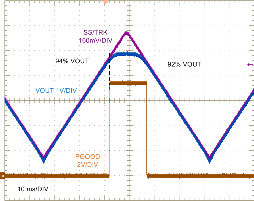 Figure 36. Typical Output Voltage Tracking and PGOOD Waveforms
Figure 36 shows a triangular voltage signal directly driving SS/TRK and the corresponding output voltage tracking response. Nominal output voltage here is 5 V, with oscilloscope channel scaling chosen such that the waveforms overlap during tracking. As expected, the PGOOD flag transitions at thresholds of 94% (rising) and 92% (falling) of the nominal output voltage setpoint.
Two practical tracking configurations, ratiometric and coincident, are shown in Figure 37. The most common application is coincident tracking, used in core versus I/O voltage tracking in DSP and FPGA implementations. Coincident tracking forces the master and slave channels to have the same output voltage ramp rate until the slave output reaches its regulated setpoint. Conversely, ratiometric tracking sets the output voltage of the slave to a fraction of the output voltage of the master during start-up.
For coincident tracking, connect the SS/TRK input of the slave regulator to a resistor divider from the output voltage of the master that is the same as the divider used on the FB pin of the slave. In other words, simply select RTRK3 = RFB3 and RTRK4 = RFB4 as shown in . As the master voltage rises, the slave voltage rises identically (aside from the 80-mV offset from SS/TRK to FB when VFB is below 0.8 V). Eventually, the slave voltage reaches its regulation voltage, at which point the internal reference takes over the regulation while the SS/TRK input continues to 115 mV above FB, and no longer controls the output voltage.
In all cases, to ensure that the output voltage accuracy is not compromised by the SS/TRK voltage being too close to the 0.8-V reference voltage, the final value of the SS/TRK voltage of the slave should be at least 100 mV above FB.
8.3.8 Voltage-Mode Control (COMP)
The LM25145 incorporates a voltage-mode control loop implementation with input voltage feedforward to eliminate the input voltage dependence of the PWM modulator gain. This configuration allows the controller to maintain stability throughout the entire input voltage operating range and provides for optimal response to input voltage transient disturbances. The constant gain provided by the controller greatly simplifies loop compensation design because the loop characteristics remain constant as the input voltage changes, unlike a buck converter without voltage feedforward. An increase in input voltage is matched by a concomitant increase in ramp voltage amplitude to maintain constant modulator gain. The input voltage feedforward gain, kFF, is 15, equivalent to the input voltage divided by the ramp amplitude, VIN/VRAMP. See Control Loop Compensation for more detail.
8.3.9 Gate Drivers (LO, HO)
The LM25145 gate driver impedances are low enough to perform effectively in high output current applications where large die-size or paralleled MOSFETs with correspondingly large gate charge, QG, are used. Measured at VVCC = 7.5 V, the low-side driver of the LM25145 has a low impedance pulldown path of 0.9 Ω to minimize the effect of dv/dt induced turnon, particularly with low gate-threshold voltage MOSFETs. Similarly, the high-side driver has 1.5-Ω and 0.9-Ω pullup and pulldown impedances, respectively, for faster switching transition times, lower switching loss, and greater efficiency.
The high-side gate driver works in conjunction with an integrated bootstrap diode and external bootstrap capacitor, CBST. When the low-side MOSFET conducts, the SW voltage is approximately at 0 V and CBST is charged from VCC through the integrated boot diode. Connect a 0.1-μF or larger ceramic capacitor close to the BST and SW pins.
Furthermore, there is a proprietary adaptive dead-time control on both switching edges to prevent shoot-through and cross-conduction, minimize body diode conduction time, and reduce body diode reverse recovery losses.
8.3.10 Current Sensing and Overcurrent Protection (ILIM)
The LM25145 implements a lossless current sense scheme designed to limit the inductor current during an overload or short-circuit condition. Figure 38 portrays the popular current sense method using the on-state resistance of the low-side MOSFET. Meanwhile, Figure 39 shows an alternative implementation with current shunt resistor, RS. The LM25145 senses the inductor current during the PWM off-time (when LO is high).
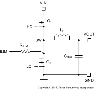 Figure 38. MOSFET RDS(on) Current Sensing
 Figure 39. Shunt Resistor Current Sensing
The ILIM pin of the LM25145 sources a reference current that flows in an external resistor, designated RILIM, to program of the current limit threshold. A current limit comparator on the ILIM pin prevents further SW pulses if the ILIM pin voltage goes below GND. Figure 40 shows the implementation.
Resistor RILIM is tied to SW to use the RDS(on) of the low-side MOSFET as a sensing element (termed RDS-ON mode). Alternatively, RILIM is tied to a shunt resistor connected at the source of the low-side MOSFET (termed RSENSE mode). The LM25145 detects the appropriate mode at start-up and sets the source current amplitude and temperature coefficient (TC) accordingly.
The ILIM current with RDS-ON sensing is 200 µA at 27°C junction temperature and incorporates a TC of +4500 ppm/°C to generally track the RDS(on) temperature variation of the low-side MOSFET. Conversely, the ILIM current is a constant 100 µA in RSENSE mode. This controls the valley of the inductor current during a steady-state overload at the output. Depending on the chosen mode, select the resistance of RILIM using Equation 6.

where
- ΔIL is the peak-to-peak inductor ripple current
- RDS(on)Q2 is the on-state resistance of the low-side MOSFET
- IRDSON is the ILIM pin current in RDS-ON mode
- RS is the resistance of the current-sensing shunt element, and
- IRS is the ILIM pin current in RSENSE mode.
Given the large voltage swings of ILIM in RDS-ON mode, a capacitor designated CILIM connected from ILIM to PGND is essential to the operation of the valley current limit circuit. Choose this capacitance such that the time constant RILIM · CILIM is approximately 6 ns.
 Figure 40. OCP Setpoint Defined by Current Source IRDSON and Resistor RILIM in RDS-ON Mode
Note that current sensing with a shunt component is typically implemented at lower output current levels to provide accurate overcurrent protection. Burdened by the unavoidable efficiency penalty, PCB layout, and additional cost implications, this configuration is not usually implemented in high-current applications (except where OCP setpoint accuracy and stability over the operating temperature range are critical specifications).
8.3.11 OCP Duty Cycle Limiter
 Figure 41. OCP Duty Cycle Limiting Waveforms
In addition to valley current limiting, the LM25145 uses a proprietary duty-cycle limiter circuit to reduce the PWM on-time during an overcurrent condition. As shown in Figure 40, an auxiliary PWM comparator along with a modulated CLAMP voltage limits how quickly the on-time increases in response to a large step in the COMP voltage that typically occurs with a voltage-mode control loop architecture.
As depicted in Figure 41, the CLAMP voltage, VCLAMP, is normally regulated above the COMP voltage to provide adequate headroom during a response to a load-on transient. If the COMP voltage rises quickly during an overloaded or shorted output condition, the on-time pulse terminates thereby limiting the on-time and peak inductor current. Moreover, the CLAMP voltage is reduced if additional valley current limit events occur, further reducing the average output current.
If the overcurrent condition exists for 128 continuous clock cycles, a hiccup event is triggered and SS is pulled low for 8192 clock cycles before a soft-start sequence is initiated.
8.4 Device Functional Modes
8.4.1 Shutdown Mode
The EN/UVLO pin provides ON / OFF control for the LM25145. When the EN/UVLO voltage is below 0.37 V (typical), the device is in shutdown mode. Both the internal bias supply LDO and the switching regulator are off. The quiescent current in shutdown mode drops to 13.5 μA (typical) at VIN = 24 V. The LM25145 also includes undervoltage protection of the internal bias LDO. If the internal bias supply voltage is below its UVLO threshold level, the switching regulator remains off.
8.4.2 Standby Mode
The internal bias supply LDO has a lower enable threshold than the switching regulator. When the EN/UVLO voltage exceeds 0.42 V (typical) and is below the precision enable threshold (1.2 V typically), the internal LDO is on and regulating. Switching action and output voltage regulation are disabled in standby mode.
8.4.3 Active Mode
The LM25145 is in active mode when the VCC voltage is above its rising UVLO threshold of 5 V and the EN/UVLO voltage is above the precision EN threshold of 1.2 V. The simplest way to enable the LM25145 is to tie EN/UVLO to VIN. This allows self start-up of the LM25145 when the input voltage exceeds the VCC threshold plus the LDO dropout voltage from VIN to VCC.
8.4.4 Diode Emulation Mode
The LM25145 provides a diode emulation feature that can be enabled to prevent reverse (drain-to-source) current flow in the low-side MOSFET. When configured for diode emulation, the low-side MOSFET is switched off when reverse current flow is detected by sensing of the SW voltage using a zero-cross comparator. The benefit of this configuration is lower power loss at no-load and light-load conditions, the disadvantage being slower light-load transient response.
The diode emulation feature is configured with the SYNCIN pin. To enable diode emulation and thus achieve discontinuous conduction mode (DCM) operation at light loads, connect the SYNCIN pin to AGND or leave SYNCIN floating. If forced PWM (FPWM) continuous conduction mode (CCM) operation is desired, tie SYNCIN to VCC either directly or using a pullup resistor. Note that diode emulation mode is automatically engaged to prevent reverse current flow during a prebias start-up. A gradual change from DCM to CCM operation provides monotonic start-up performance.
8.4.5 Thermal Shutdown
The LM25145 includes an internal junction temperature monitor. If the temperature exceeds 175°C (typical), thermal shutdown occurs.
When entering thermal shutdown, the device:
- Turns off the low-side and high-side MOSFETs;
- Pulls SS/TRK and PGOOD low;
- Initiates a soft-start sequence when the die temperature decreases by the thermal shutdown hysteresis of 20°C (typical).