ZHCSGE8A June 2017 – August 2018 UCC27712
PRODUCTION DATA.
- 1 特性
- 2 应用
- 3 说明
- 4 修订历史记录
- 5 Pin Configuration and Functions
- 6 Specifications
- 7 Detailed Description
-
8 Application and Implementation
- 8.1 Application Information
- 8.2
Typical Application
- 8.2.1 Design Requirements
- 8.2.2
Detailed Design Procedure
- 8.2.2.1 Selecting HI and LI Low Pass Filter Components (RHI, RLI, CHI, CLI)
- 8.2.2.2 Selecting Bootstrap Capacitor (CBOOT)
- 8.2.2.3 Selecting VDD Bypass/Holdup Capacitor (CVDD) and Rbias
- 8.2.2.4 Selecting Bootstrap Resistor (RBOOT)
- 8.2.2.5 Selecting Gate Resistor RON/ROFF
- 8.2.2.6 Selecting Bootstrap Diode
- 8.2.2.7 Estimate the UCC27712 Power Losses (PUCC27712)
- 8.2.2.8 Estimating Junction Temperature
- 8.2.2.9 Operation With IGBT's
- 8.2.3 Application Curves
- 9 Power Supply Recommendations
- 10Layout
- 11器件和文档支持
- 12机械、封装和可订购信息
7.3.1 VDD and Under Voltage Lockout
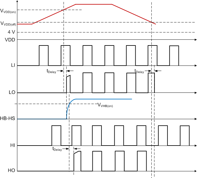
The UCC27712 has an internal under voltage-lockout (UVLO) protection feature on the supply circuit blocks between VDD and VSS pins, as well as between HB and HS pins. When VDD bias voltage is lower than the VVDD(on) threshold at device start-up or lower than VVDD(off) after start-up, the VDD UVLO feature holds both the LO and HO outputs low, regardless of the status of the HI and LI inputs. On the other hand, if HB-HS bias supply voltage is lower than the VVHB(on) threshold at start-up or VVHB(off) after start-up, the HB-HS UVLO feature only holds HO to low, regardless of the status of the HI. The LO output status is not affected by the HB-HS UVLO feature (see Table 1 and Table 2). This allows the LO output to turn-on and re-charge the HB-HS capacitor using the boot-strap circuit and thus allows HB-HS bias voltage to surpass the VVHB(on) threshold.
Both the VDD and VHB UVLO protection functions are provided with a hysteresis feature. This hysteresis prevents chatter when there is ground noise from the power supply. Also this allows the device to accept a small drop in the bias voltage which is bound to happen when the device starts switching and quiescent current consumption increases instantaneously, as well as when the boot-strap circuit charges the HB-HS capacitor during the first instance of LO turn-on causing a drop in VDD voltage.
The UVLO circuit of VDD-VSS and HB-HS in UCC27712 generate internal signals to enable/disable the outputs after UVLO_ON/UVLO_OFF thresholds are crossed respectively (please refer to Figure 30). Design considerations indicate that the UVLO propagation delay before the outputs are enabled and disabled can vary from 20 μs to 50 μs.
Table 1. VDD UVLO Feature Logic Operation
| CONDITION (VHB-VHS>VVHB, ON FOR ALL CASES BELOW) | HI | LI | HO | LO |
|---|---|---|---|---|
| VDD-VSS < VVDD(on) during device start up | H | L | L | L |
| VDD-VSS < VVDD(on) during device start up | L | H | L | L |
| VDD-VSS < VVDD(on) during device start up | H | H | L | L |
| VDD-VSS < VVDD(on) during device start up | L | L | L | L |
| VDD-VSS < VVDD(off) after device start up | H | L | L | L |
| VDD-VSS < VVDD(off) after device start up | L | H | L | L |
| VDD-VSS < VVDD(off) after device start up | H | H | L | L |
| VDD-VSS < VVDD(off) after device start up | L | L | L | L |
Table 2. VHB UVLO Feature Logic Operation
| CONDITION (VDD-VSS > VVDD,ON FOR ALL CASES BELOW) | HI | LI | HO | LO |
|---|---|---|---|---|
| VHB-VHS < VVHB(on) during device start up | H | L | L | L |
| VHB-VHS < VVHB(on) during device start up | L | H | L | H |
| VHB-VHS < VVHB(on) during device start up | H | H | L | L |
| VHB-VHS < VVHB(on) during device start up | L | L | L | L |
| VHB-VHS < VVHB(off) after device start up | H | L | L | L |
| VHB-VHS < VVHB(off) after device start up | L | H | L | H |
| VHB-VHS < VVHB(off) after device start up | H | H | L | L |
| VHB-VHS < VVHB(off) after device start up | L | L | L | L |
 Figure 30. Power-Up Driver