ZHCSGF2C July   2017  – June 2019 TLV743P

PRODUCTION DATA.  

  1. 特性
  2. 应用
  3. 说明
    1.     Device Images
      1.      典型应用电路
      2.      压降电压与输出电流间的关系
  4. 修订历史记录
  5. Pin Configuration and Functions
    1.     Pin Functions
  6. Specifications
    1. 6.1 Absolute Maximum Ratings
    2. 6.2 ESD Ratings
    3. 6.3 Recommended Operating Conditions
    4. 6.4 Thermal Information
    5. 6.5 Electrical Characteristics
    6. 6.6 Typical Characteristics
  7. Detailed Description
    1. 7.1 Overview
    2. 7.2 Functional Block Diagram
    3. 7.3 Feature Description
      1. 7.3.1 Undervoltage Lockout (UVLO)
      2. 7.3.2 Shutdown and Output Enable
      3. 7.3.3 Internal Foldback Current Limit
      4. 7.3.4 Thermal Shutdown
    4. 7.4 Device Functional Modes
      1. 7.4.1 Normal Operation
      2. 7.4.2 Dropout Operation
      3. 7.4.3 Disabled
  8. Application and Implementation
    1. 8.1 Application Information
      1. 8.1.1 Input and Output Capacitor Selection
      2. 8.1.2 Dropout Voltage
      3. 8.1.3 Power Dissipation
    2. 8.2 Typical Application
      1. 8.2.1 Design Requirements
      2. 8.2.2 Detailed Design Procedure
      3. 8.2.3 Application Curve
  9. Power Supply Recommendations
  10. 10Layout
    1. 10.1 Layout Guidelines
    2. 10.2 Layout Examples
  11. 11器件和文档支持
    1. 11.1 器件支持
      1. 11.1.1 开发支持
        1. 11.1.1.1 评估模块
      2. 11.1.2 器件命名规则
    2. 11.2 文档支持
      1. 11.2.1 相关文档
    3. 11.3 接收文档更新通知
    4. 11.4 社区资源
    5. 11.5 商标
    6. 11.6 静电放电警告
    7. 11.7 Glossary
  12. 12机械、封装和可订购信息

Typical Characteristics

at operating temperature range (TJ = –40°C to +125°C), VIN = VOUT(nom) + 0.5 V or 2 V (whichever is greater), IOUT = 1 mA, VEN = VIN, and CIN = COUT = 1 µF (unless otherwise noted)
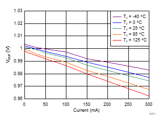
TLV743P D001_sbvs235.gif
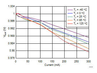
TLV74310PDBV
Figure 1. 1-V Load Regulation vs IOUT and Temperature
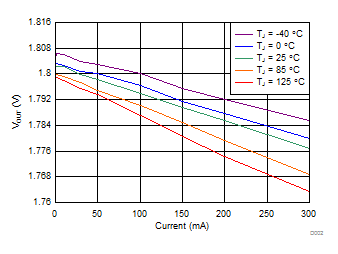
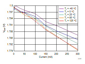
TLV743P D002_sbvs235.gif
TLV74318PDBV
Figure 3. 1.8-V Load Regulation vs IO and Temperature
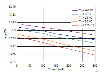
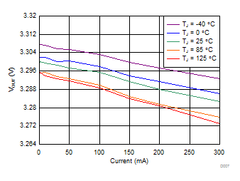
TLV743P D003_sbvs235.gif
TLV74333PDBV
Figure 5. 3.3-V Load Regulation vs IOUT and Temperature
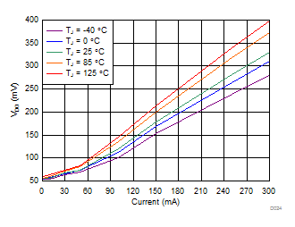
TLV743P D024_sbvs235.gif
TLV74312PDBV
Figure 7. 1.2-V Dropout Voltage vs IOUT and Temperature
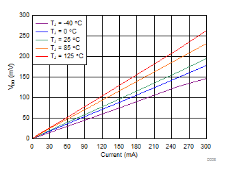
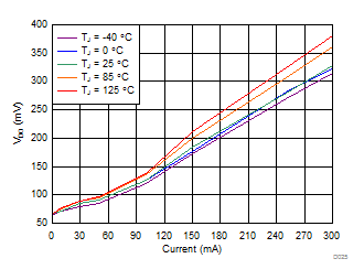
TLV743P D008_sbvs235.gif
TLV74318PDBV
Figure 9. 1.8-V Dropout Voltage vs IOUT and Temperature
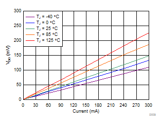
TLV743P D009_sbvs235.gif
TLV74333PDBV
Figure 11. 3.3-V Dropout Voltage vs IOUT and Temperature
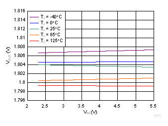
TLV743P D019_sbvs235.gif
TLV74318PDBV
Figure 13. 1.8-V Regulation vs VIN (Line Regulation) and Temperature
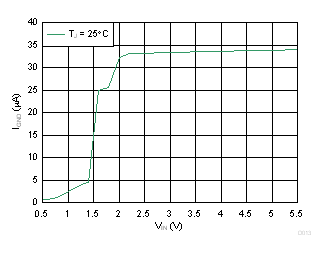
TLV743P D013_sbvs235.gif
Figure 15. Ground Pin Current vs VIN
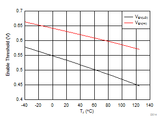
TLV743P D014_sbvs235.gif
Figure 17. Enable Threshold vs Temperature
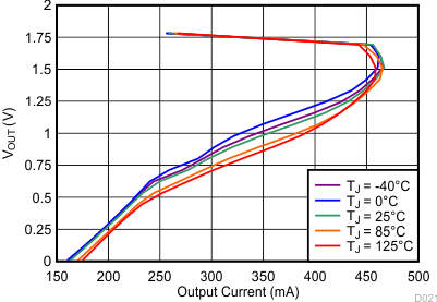
TLV743P D021_sbvs235.gif
TLV74318PDBV
Figure 19. 1.8-V Foldback Current Limit vs
IOUT and Temperature
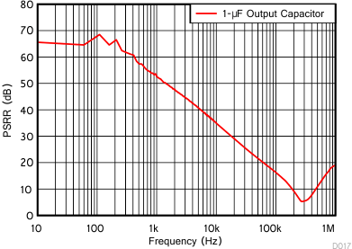
TLV743P D017_sbvs235.gif
IOUT = 300 mA
Figure 21. Power-Supply Rejection Ratio vs Frequency
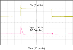
TLV743P LineTrans10mA.gif
TLV74318PDBV, IOUT = 10 mA, 1-µF output capacitor
Figure 23. Line Transient
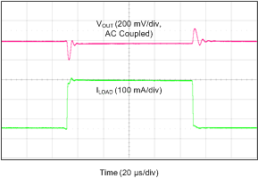
TLV743P LoadTranswcap1p0.gif
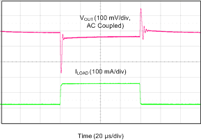
TLV74310PDBV VIN = 2 V, 1-µF output capacitor, output current slew rate = 0.25 A/µs
Figure 25. 1-V, 50-mA to 300-mA Load Transient
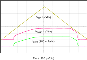
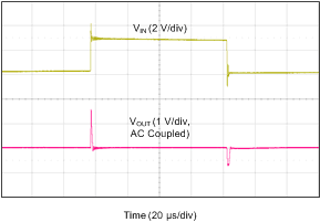
TLV743P Triangle.gif
TLV74318PDBV, RL = 6.2 Ω, VEN = VIN, 1-µF output capacitor
Figure 27. VIN Power-Up and Power-Down
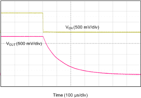
TLV743P Shutdown.gif
TLV74318PDBV, IOUT = 300 mA, 1-µF output capacitor
Figure 29. Shutdown Response With Enable
TLV743P D005_sbvs235.gif
TLV74310PDQN
Figure 2. 1-V Load Regulation vs IOUT and Temperature
TLV743P D006_sbvs235.gif
TLV74318PDQN
Figure 4. 1.8-V Load Regulation vs IOUT and Temperature
TLV743P D007_sbvs235.gif
TLV74333PDQN
Figure 6. 3.3-V Load Regulation vs IOUT and Temperature
TLV743P D025_sbvs235.gif
TLV74312PDQN
Figure 8. 1.2-V Dropout Voltage vs IOUT and Temperature
TLV743P D010_sbvs235.gif
TLV74318PDQN
Figure 10. 1.8-V Dropout Voltage vs IOUT and Temperature
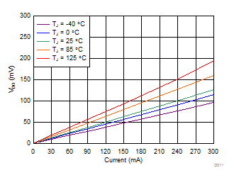
TLV743P D011_sbvs235.gif
TLV74333PDQN
Figure 12. 3.3-V Dropout Voltage vs IOUT and Temperature
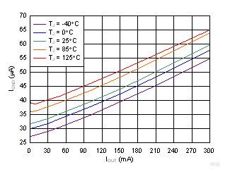
TLV743P D012_sbvs235.gif
Figure 14. Ground Pin Current vs IOUT and Temperature
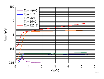
TLV743P D015_sbvs235.gif
IOUT = 0 mA
Figure 16. Shutdown Current vs VIN and Temperature
TLV743P D023_sbvs235.gif
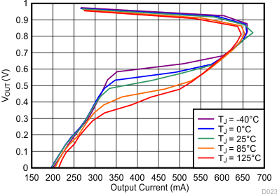
TLV74310PDBV
Figure 18. 1-V Foldback Current Limit vs
IOUT and Temperature
TLV743P D022_sbvs235.gif
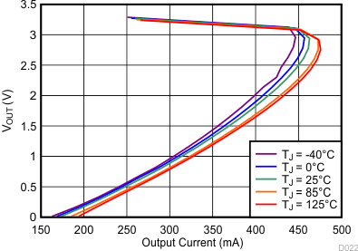
TLV74333PDBV
Figure 20. 3.3-V Foldback Current Limit vs
IOUT and Temperature
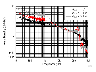
TLV743P D016_sbvs235.gif
IOUT = 300 mA
Figure 22. Output Spectral Noise Density
TLV743P LineTrans300mA.gif
TLV74318PDBV IOUT = 300 mA 1-µF output capacitor
Figure 24. Line Transient
TLV743P LoadTranswcap.gif
TLV74333PDBV, VIN = 3.8 V,1-µF output capacitor, output current slew rate = 0.25 A/µs
Figure 26. 3.3 V, 50-mA to 300-mA Load Transient
TLV743P Enstartup1p8.gif
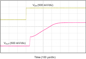
TLV74318PDBV, RL = 6.2 Ω, 1-µF output capacitor
Figure 28. Startup with EN
TLV743P Current_Limit.gif
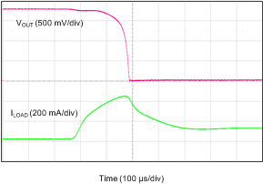
TLV74318PDBV, 1-µF output capacitor
Figure 30. Foldback Current Limit Response