ZHCSGF2C July 2017 – June 2019 TLV743P
PRODUCTION DATA.
8.1.3 Power Dissipation
The ability to remove heat from the die is different for each package type and presents different considerations in the printed circuit board (PCB) layout. The PCB area around the device that is free of other components moves the heat from the device to ambient air. Performance data for JEDEC high-K boards are shown in Thermal Information. Using heavier copper increases the effectiveness in removing heat from the device. The addition of plated through-holes to heat-dissipating layers also improves heat sink effectiveness.
Power dissipation (PD) depends on input voltage and load conditions. PD is equal to the product of the output current and voltage drop across the output pass element, as shown in Equation 2.

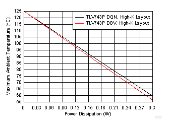
Figure 31 shows the maximum ambient temperature versus the power dissipation of the TLV743P device in the DQN and DBV packages. This figure assumes the device is soldered on JEDEC standard high-K layout with no airflow over the board. Actual board thermal impedances vary widely. If the application requires high power dissipation, it is helpful to have a thorough understanding of the board temperature and thermal impedances to make certain that the TLV743P device does not operate continuously above a junction temperature of 125°C.
