ZHCSGI8A April   2017  – October 2021 ADC12D1620QML-SP

PRODUCTION DATA  

  1. 特性
  2. 应用
  3. 说明
  4. Revision History
  5. Pin Configuration and Functions
  6. Specifications
    1. 6.1  Absolute Maximum Ratings
    2. 6.2  ESD Ratings
    3. 6.3  Recommended Operating Conditions
    4. 6.4  Thermal Information
    5. 6.5  Converter Electrical Characteristics: Static Converter Characteristics
    6. 6.6  Converter Electrical Characteristics: Dynamic Converter Characteristics
    7. 6.7  Converter Electrical Characteristics: Analog Input/Output and Reference Characteristics
    8. 6.8  Converter Electrical Characteristic: Channel-to-Channel Characteristics
    9. 6.9  Converter Electrical Characteristics: LVDS CLK Input Characteristics
    10. 6.10 Electrical Characteristics: AutoSync Feature
    11. 6.11 Converter Electrical Characteristics: Digital Control and Output Pin Characteristics
    12. 6.12 Converter Electrical Characteristics: Power Supply Characteristics
    13. 6.13 Converter Electrical Characteristics: AC Electrical Characteristics
    14. 6.14 Electrical Characteristics: Delta Parameters
    15. 6.15 Timing Requirements: Serial Port Interface
    16. 6.16 Timing Requirements: Calibration
    17. 6.17 Quality Conformance Inspection
    18. 6.18 Timing Diagrams
    19. 6.19 Typical Characteristics
  7. Detailed Description
    1. 7.1 Overview
      1. 7.1.1 Operation Summary
    2. 7.2 Functional Block Diagram
    3. 7.3 Feature Description
      1. 7.3.1 Input Control and Adjust
        1. 7.3.1.1 AC- and DC-Coupled Modes
        2. 7.3.1.2 Input Full-Scale Range Adjust
        3. 7.3.1.3 Input Offset Adjust
        4. 7.3.1.4 Low-Sampling Power-Saving Mode (LSPSM)
        5. 7.3.1.5 DES Timing Adjust
        6. 7.3.1.6 Sampling Clock Phase Adjust
      2. 7.3.2 Output Control and Adjust
        1. 7.3.2.1 SDR / DDR Clock
        2. 7.3.2.2 LVDS Output Differential Voltage
        3. 7.3.2.3 LVDS Output Common-Mode Voltage
        4. 7.3.2.4 Output Formatting
        5. 7.3.2.5 Test-Pattern Mode
        6. 7.3.2.6 Time Stamp
      3. 7.3.3 Calibration Feature
        1. 7.3.3.1 Calibration Control Pins and Bits
        2. 7.3.3.2 How to Execute a Calibration
        3. 7.3.3.3 On-Command Calibration
        4. 7.3.3.4 Calibration Adjust
          1. 7.3.3.4.1 Read/Write Calibration Settings
        5. 7.3.3.5 Calibration and Power-Down
        6. 7.3.3.6 Calibration and the Digital Outputs
      4. 7.3.4 Power Down
      5. 7.3.5 Low-Sampling Power-Saving Mode (LSPSM)
    4. 7.4 Device Functional Modes
      1. 7.4.1 DES/Non-DES Mode
      2. 7.4.2 Demux/Non-Demux Mode
    5. 7.5 Programming
      1. 7.5.1 Control Modes
        1. 7.5.1.1 Non-ECM
          1. 7.5.1.1.1  Dual-Edge Sampling Pin (DES)
          2. 7.5.1.1.2  Non-Demultiplexed Mode Pin (NDM)
          3. 7.5.1.1.3  Dual Data-Rate Phase Pin (DDRPh)
          4. 7.5.1.1.4  Calibration Pin (CAL)
          5. 7.5.1.1.5  Low-Sampling Power-Saving Mode Pin (LSPSM)
          6. 7.5.1.1.6  Power-Down I-Channel Pin (PDI)
          7. 7.5.1.1.7  Power-Down Q-Channel Pin (PDQ)
          8. 7.5.1.1.8  Test-Pattern Mode Pin (TPM)
          9. 7.5.1.1.9  Full-Scale Input-Range Pin (FSR)
          10. 7.5.1.1.10 AC- or DC-Coupled Mode Pin (VCMO)
          11. 7.5.1.1.11 LVDS Output Common-Mode Pin (VBG)
        2. 7.5.1.2 Extended Control Mode
          1. 7.5.1.2.1 Serial Interface
    6. 7.6 Register Maps
      1. 7.6.1 Register Definitions
  8. Application Information Disclaimer
    1. 8.1 Application Information
      1. 8.1.1 Analog Inputs
        1. 8.1.1.1 Acquiring the Input
        2. 8.1.1.2 Driving the ADC in DES Mode
        3. 8.1.1.3 FSR and the Reference Voltage
        4. 8.1.1.4 Out-Of-Range Indication
        5. 8.1.1.5 AC-Coupled Input Signals
        6. 8.1.1.6 DC-Coupled Input Signals
        7. 8.1.1.7 Single-Ended Input Signals
      2. 8.1.2 Clock Inputs
        1. 8.1.2.1 CLK Coupling
        2. 8.1.2.2 CLK Frequency
        3. 8.1.2.3 CLK Level
        4. 8.1.2.4 CLK Duty Cycle
        5. 8.1.2.5 CLK Jitter
        6. 8.1.2.6 CLK Layout
      3. 8.1.3 LVDS Outputs
        1. 8.1.3.1 Common-Mode and Differential Voltage
        2. 8.1.3.2 Output Data Rate
        3. 8.1.3.3 Terminating Unused LVDS Output Pins
      4. 8.1.4 Synchronizing Multiple ADC12D1620 Devices in a System
        1. 8.1.4.1 AutoSync Feature
        2. 8.1.4.2 DCLK Reset Feature
      5. 8.1.5 Temperature Sensor
    2. 8.2 Radiation Environments
      1. 8.2.1 Total Ionizing Dose
      2. 8.2.2 Single Event Latch-Up and Functional Interrupt
      3. 8.2.3 Single Event Upset
    3. 8.3 Cold Sparing
  9. Power Supply Recommendations
    1. 9.1 System Power-On Considerations
      1. 9.1.1 Control Pins
      2. 9.1.2 Power On in Non-ECM
      3. 9.1.3 Power On in ECM
      4. 9.1.4 Power-on and Data Clock (DCLK)
  10. 10Layout
    1. 10.1 Layout Guidelines
      1. 10.1.1 Power Planes
      2. 10.1.2 Bypass Capacitors
      3. 10.1.3 Ground Planes
      4. 10.1.4 Power System Example
    2. 10.2 Layout Example
    3. 10.3 Thermal Considerations
    4. 10.4 Board Mounting Recommendation
  11. 11Device and Documentation Support
    1. 11.1 Device Support
      1. 11.1.1 Device Nomenclature
      2. 11.1.2 第三方米6体育平台手机版_好二三四免责声明
    2. 11.2 接收文档更新通知
    3. 11.3 支持资源
    4. 11.4 Trademarks
    5. 11.5 静电放电警告
    6. 11.6 术语表
  12. 12Mechanical, Packaging, and Orderable Information
    1. 12.1 Engineering Samples

AC-Coupled Input Signals

The ADC12D1620 analog inputs require a precise common-mode voltage. This voltage is generated on-chip when AC-coupling mode is selected. See AC- and DC-Coupled Modes for more information about how to select AC-coupled mode.

In AC-coupled mode, the analog inputs must of course be AC-coupled. For an ADC12D1620 used in a typical application, this may be accomplished by on-board capacitors, as shown in Figure 8-2.

When the AC-coupled mode is selected, terminate unused channels as shown in Table 8-1. Do not connect an unused analog input directly to ground.
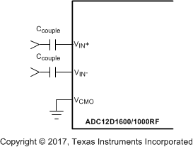
GUID-EAAE6957-7DB1-4054-AA72-5BA4C5B10AED-low.gifFigure 8-2 AC-Coupled Differential Input

The analog inputs for the ADC12D1620 are internally buffered; this simplifies the task of driving these inputs and the RC pole, which is generally used at sampling ADC inputs, is not required. If the user desires to place an amplifier circuit before the ADC, take care to choose an amplifier with adequate noise and distortion performance, and adequate gain at the frequencies used for the application.