ZHCSGJ8B April   2017  – October 2017 LM36010

PRODUCTION DATA.  

  1. 特性
  2. 应用
  3. 说明
    1.     Device Images
      1.      简化电路原理图
  4. 修订历史记录
  5. Pin Configuration and Functions
    1.     Pin Functions
  6. Specifications
    1. 6.1 Absolute Maximum Ratings
    2. 6.2 ESD Ratings
    3. 6.3 Recommended Operating Conditions
    4. 6.4 Thermal Information
    5. 6.5 Electrical Characteristics
    6. 6.6 Timing Requirements
    7. 6.7 Switching Characteristics
    8. 6.8 Typical Characteristics
  7. Detailed Description
    1. 7.1 Overview
    2. 7.2 Functional Block Diagram
    3. 7.3 Feature Description
      1. 7.3.1 Flash Mode
      2. 7.3.2 Torch Mode
      3. 7.3.3 IR Mode
    4. 7.4 Device Functioning Modes
      1. 7.4.1 Start-Up (Enabling The Device)
      2. 7.4.2 Pass Mode
      3. 7.4.3 Input Voltage Flash Monitor (IVFM)
      4. 7.4.4 Fault/Protections
        1. 7.4.4.1 Overvoltage Protection (OVP)
        2. 7.4.4.2 Input Voltage Flash Monitor (IVFM)
        3. 7.4.4.3 LED and/or VOUT Short Fault
        4. 7.4.4.4 Current Limit (OCP)
        5. 7.4.4.5 Thermal Scale-Back (TSB)
        6. 7.4.4.6 Thermal Shutdown (TSD)
        7. 7.4.4.7 Undervoltage Lockout (UVLO)
        8. 7.4.4.8 Flash Time-out (FTO)
    5. 7.5 Programming
      1. 7.5.1 Control Truth Table
      2. 7.5.2 I2C-Compatible Interface
        1. 7.5.2.1 Data Validity
        2. 7.5.2.2 Start and Stop Conditions
        3. 7.5.2.3 Transferring Data
        4. 7.5.2.4 I2C-Compatible Chip Address
    6. 7.6 Register Descriptions
      1. 7.6.1 Enable Register (0x01)
      2. 7.6.2 Configuration Register (0x02)
      3. 7.6.3 LED Flash Brightness Register (0x03)
      4. 7.6.4 LED Torch Brightness Register (0x04)
      5. 7.6.5 Flags Register (0x05)
      6. 7.6.6 Device ID and RESET Register (0x06)
  8. Applications and Implementation
    1. 8.1 Application Information
    2. 8.2 Typical Application
      1. 8.2.1 Design Requirements
      2. 8.2.2 Detailed Design Procedure
        1. 8.2.2.1 Thermal Performance
        2. 8.2.2.2 Output Capacitor Selection
        3. 8.2.2.3 Input Capacitor Selection
        4. 8.2.2.4 Inductor Selection
      3. 8.2.3 Application Curves
  9. Power Supply Recommendations
  10. 10Layout
    1. 10.1 Layout Guidelines
    2. 10.2 Layout Example
  11. 11器件和文档支持
    1. 11.1 器件支持
      1. 11.1.1 Third-Party Products Disclaimer
    2. 11.2 文档支持
      1. 11.2.1 相关文档
    3. 11.3 接收文档更新通知
    4. 11.4 社区资源
    5. 11.5 商标
    6. 11.6 静电放电警告
    7. 11.7 Glossary
  12. 12机械、封装和可订购信息

Transferring Data

Every byte put on the SDA line must be eight bits long, with the most significant bit (MSB) transferred first. Each byte of data has to be followed by an acknowledge bit. The acknowledge related clock pulse is generated by the master. The master releases the SDA line (HIGH) during the acknowledge clock pulse. The LM36010 pulls down the SDA line during the 9th clock pulse, signifying an acknowledge. The LM36010 generates an acknowledge after each byte is received. There is no acknowledge created after data is read from the device.

After the START condition, the I2C master sends a chip address. This address is seven bits long followed by an eighth bit which is a data direction bit (R/W). The LM36010 7-bit address is 0x64. For the eighth bit, a 0 indicates a WRITE, and a 1 indicates a READ. The second byte selects the register to which the data is written. The third byte contains data to write to the selected register.
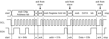
LM36010 I2CwriteEX.gifFigure 35. Write Cycle W = Write (SDA = 0) R = Read (SDA = 1) Ack = Acknowledge
(SDA Pulled Down by Either Master or Slave) ID = Chip Address, 64h for LM36010