ZHCSGJ8B April   2017  – October 2017 LM36010

PRODUCTION DATA.  

  1. 特性
  2. 应用
  3. 说明
    1.     Device Images
      1.      简化电路原理图
  4. 修订历史记录
  5. Pin Configuration and Functions
    1.     Pin Functions
  6. Specifications
    1. 6.1 Absolute Maximum Ratings
    2. 6.2 ESD Ratings
    3. 6.3 Recommended Operating Conditions
    4. 6.4 Thermal Information
    5. 6.5 Electrical Characteristics
    6. 6.6 Timing Requirements
    7. 6.7 Switching Characteristics
    8. 6.8 Typical Characteristics
  7. Detailed Description
    1. 7.1 Overview
    2. 7.2 Functional Block Diagram
    3. 7.3 Feature Description
      1. 7.3.1 Flash Mode
      2. 7.3.2 Torch Mode
      3. 7.3.3 IR Mode
    4. 7.4 Device Functioning Modes
      1. 7.4.1 Start-Up (Enabling The Device)
      2. 7.4.2 Pass Mode
      3. 7.4.3 Input Voltage Flash Monitor (IVFM)
      4. 7.4.4 Fault/Protections
        1. 7.4.4.1 Overvoltage Protection (OVP)
        2. 7.4.4.2 Input Voltage Flash Monitor (IVFM)
        3. 7.4.4.3 LED and/or VOUT Short Fault
        4. 7.4.4.4 Current Limit (OCP)
        5. 7.4.4.5 Thermal Scale-Back (TSB)
        6. 7.4.4.6 Thermal Shutdown (TSD)
        7. 7.4.4.7 Undervoltage Lockout (UVLO)
        8. 7.4.4.8 Flash Time-out (FTO)
    5. 7.5 Programming
      1. 7.5.1 Control Truth Table
      2. 7.5.2 I2C-Compatible Interface
        1. 7.5.2.1 Data Validity
        2. 7.5.2.2 Start and Stop Conditions
        3. 7.5.2.3 Transferring Data
        4. 7.5.2.4 I2C-Compatible Chip Address
    6. 7.6 Register Descriptions
      1. 7.6.1 Enable Register (0x01)
      2. 7.6.2 Configuration Register (0x02)
      3. 7.6.3 LED Flash Brightness Register (0x03)
      4. 7.6.4 LED Torch Brightness Register (0x04)
      5. 7.6.5 Flags Register (0x05)
      6. 7.6.6 Device ID and RESET Register (0x06)
  8. Applications and Implementation
    1. 8.1 Application Information
    2. 8.2 Typical Application
      1. 8.2.1 Design Requirements
      2. 8.2.2 Detailed Design Procedure
        1. 8.2.2.1 Thermal Performance
        2. 8.2.2.2 Output Capacitor Selection
        3. 8.2.2.3 Input Capacitor Selection
        4. 8.2.2.4 Inductor Selection
      3. 8.2.3 Application Curves
  9. Power Supply Recommendations
  10. 10Layout
    1. 10.1 Layout Guidelines
    2. 10.2 Layout Example
  11. 11器件和文档支持
    1. 11.1 器件支持
      1. 11.1.1 Third-Party Products Disclaimer
    2. 11.2 文档支持
      1. 11.2.1 相关文档
    3. 11.3 接收文档更新通知
    4. 11.4 社区资源
    5. 11.5 商标
    6. 11.6 静电放电警告
    7. 11.7 Glossary
  12. 12机械、封装和可订购信息

Pin Configuration and Functions

YKB Package
8-Pin DSBGA
Top View
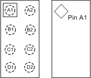
LM36010 pinout.gif

Pin Functions

PINTYPE(1)DESCRIPTION
NAMENO.
A1 GND G Ground
A2 IN P Input voltage connection. Connect IN to the input supply and bypass to GND with a 10-µF or larger ceramic capacitor.
B1 SW P Drain connection for Internal NMOS and synchronous PMOS switches.
B2 STROBE I Active high hardware flash enable. Drive STROBE high to turn on flash pulse. An internal pulldown resistor of 300 kΩ is between STROBE and GND.
C1 OUT P Step-up DC-DC converter output. Connect a 10-µF ceramic capacitor between this terminal and GND.
C2 SDA I/O I2C serial data input/output.
D1 LED P High-side current source output for flash LED.
D2 SCL I I2C serial clock input.
G = Ground; P = Power; I = Input; O = Output