ZHCSGK0H August   2017  – January 2024 ISO7760 , ISO7761 , ISO7762 , ISO7763

PRODUCTION DATA  

  1.   1
  2. 特性
  3. 应用
  4. 说明
  5. Pin Configuration and Functions
  6. Specifications
    1. 5.1  Absolute Maximum Ratings
    2. 5.2  ESD Ratings
    3. 5.3  Recommended Operating Conditions
    4. 5.4  Thermal Information
    5. 5.5  Power Ratings
    6. 5.6  Insulation Specifications
    7. 5.7  Safety-Related Certifications
    8. 5.8  Safety Limiting Values
    9. 5.9  Electrical Characteristics—5-V Supply
    10. 5.10 Supply Current Characteristics—5-V Supply
    11. 5.11 Electrical Characteristics—3.3-V Supply
    12. 5.12 Supply Current Characteristics—3.3-V Supply
    13. 5.13 Electrical Characteristics—2.5-V Supply 
    14. 5.14 Supply Current Characteristics—2.5-V Supply
    15. 5.15 Switching Characteristics—5-V Supply
    16. 5.16 Switching Characteristics—3.3-V Supply
    17. 5.17 Switching Characteristics—2.5-V Supply
    18. 5.18 Insulation Characteristics Curves
    19. 5.19 Typical Characteristics
  7. Parameter Measurement Information
  8. Detailed Description
    1. 7.1 Overview
    2. 7.2 Functional Block Diagram
    3. 7.3 Feature Description
      1. 7.3.1 Electromagnetic Compatibility (EMC) Considerations
    4. 7.4 Device Functional Modes
      1. 7.4.1 Device I/O Schematics
  9. Application and Implementation
    1. 8.1 Application Information
    2. 8.2 Typical Application
      1. 8.2.1 Design Requirements
      2. 8.2.2 Detailed Design Procedure
      3. 8.2.3 Application Curves
        1. 8.2.3.1 Insulation Lifetime
  10. Power Supply Recommendations
  11. 10Layout
    1. 10.1 Layout Guidelines
      1. 10.1.1 PCB Material
    2. 10.2 Layout Example
  12. 11Device and Documentation Support
    1. 11.1 Documentation Support
      1. 11.1.1 Related Documentation
    2. 11.2 Receiving Notification of Documentation Updates
    3. 11.3 Community Resources
    4. 11.4 Trademarks
  13. 12Revision History
  14. 13Mechanical, Packaging, and Orderable Information

Typical Characteristics

GUID-20231115-SS0I-WZCT-9NK7-QR4C4Z3VT1RP-low.svg
TA = 25°C CL = 15 pF
Figure 5-5 ISO7760 Supply Current vs Data Rate (With 15-pF Load)
GUID-20231115-SS0I-R6WM-DWWB-NWQFVVSKQ2RH-low.svg
TA = 25°C CL = 15 pF
Figure 5-7 ISO7761 Supply Current vs Data Rate (With 15-pF Load)
GUID-20231115-SS0I-K2TJ-PQKZ-LFSVNCHQDKF7-low.svg
TA = 25°C CL = 15 pF
Figure 5-9 ISO7762 Supply Current vs Data Rate (With 15-pF Load)
GUID-20231115-SS0I-83Z0-FNQH-TNJJM710KNNJ-low.svg
TA = 25°C CL = 15 pF
Figure 5-11 ISO7763 Supply Current vs Data Rate (With 15-pF Load)
GUID-20231115-SS0I-X3QN-82HT-72WCLLMRDGSP-low.svg
TA = 25°C
Figure 5-13 High-Level Output Voltage vs High-Level Output Current
GUID-20231115-SS0I-C28H-GC9X-DJGQDSWF3KNJ-low.svg
Figure 5-15 Power Supply Undervoltage Threshold vs Free-Air Temperature
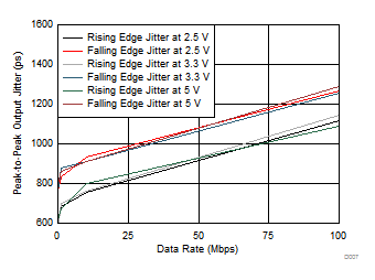
GUID-20AA97B3-004C-49FA-8D4F-E05906ABE894-low.gif
TA = 25°C
Figure 5-17 Peak-to-Peak Output Jitter vs Data Rate
GUID-20231115-SS0I-SSW8-BRRZ-CZCTL7QMCGPP-low.svg
TA = 25°C CL = No Load
Figure 5-6 ISO7760 Supply Current vs Data Rate (With No Load)
GUID-20231115-SS0I-DLCC-8RWL-SGDCWB6PCX19-low.svg
TA = 25°C CL = No Load
Figure 5-8 ISO7761 Supply Current vs Data Rate (With No Load)
GUID-20231115-SS0I-SXZD-MBFW-HNB8QNHBHN8Q-low.svg
TA = 25°C CL = No Load
Figure 5-10 ISO7762 Supply Current vs Data Rate (With No Load)
GUID-20231115-SS0I-PGQ8-QFVC-6D36DH0J0GWL-low.svg
TA = 25°C CL = No Load
Figure 5-12 ISO7763 Supply Current vs Data Rate (With No Load)
GUID-20231115-SS0I-5LKS-5NN7-2DW7LHX1MFJH-low.svg
TA = 25°C
Figure 5-14 Low-Level Output Voltage vs Low-Level Output Current
GUID-20231115-SS0I-CPPT-5R9H-GKBXDPKX9430-low.svg
Figure 5-16 Propagation Delay Time vs Free-Air Temperature