ZHCSGL2E December 2016 – December 2023 LMK62A2-100M , LMK62A2-150M , LMK62A2-156M , LMK62A2-200M , LMK62A2-266M , LMK62E0-156M , LMK62E2-100M , LMK62E2-156M , LMK62I0-100M , LMK62I0-156M
PRODUCTION DATA
- 1
- 1 特性
- 2 应用
- 3 说明
- 4 Pin Configuration and Functions
-
5 Specifications
- 5.1 Absolute Maximum Ratings
- 5.2 ESD Ratings
- 5.3 Recommended Operating Conditions
- 5.4 Thermal Information
- 5.5 Electrical Characteristics - Power Supply
- 5.6 LVPECL Output Characteristics
- 5.7 LVDS Output Characteristics
- 5.8 HCSL Output Characteristics
- 5.9 OE Input Characteristics
- 5.10 Frequency Tolerance Characteristics
- 5.11 Power-On/Reset Characteristics (VDD)
- 5.12 PSRR Characteristics
- 5.13 PLL Clock Output Jitter Characteristics
- 5.14 Additional Reliability and Qualification
- 6 Parameter Measurement Information
- 7 Application and Implementation
- 8 Device and Documentation Support
- 9 Revision History
- 10Mechanical, Packaging, and Orderable Information
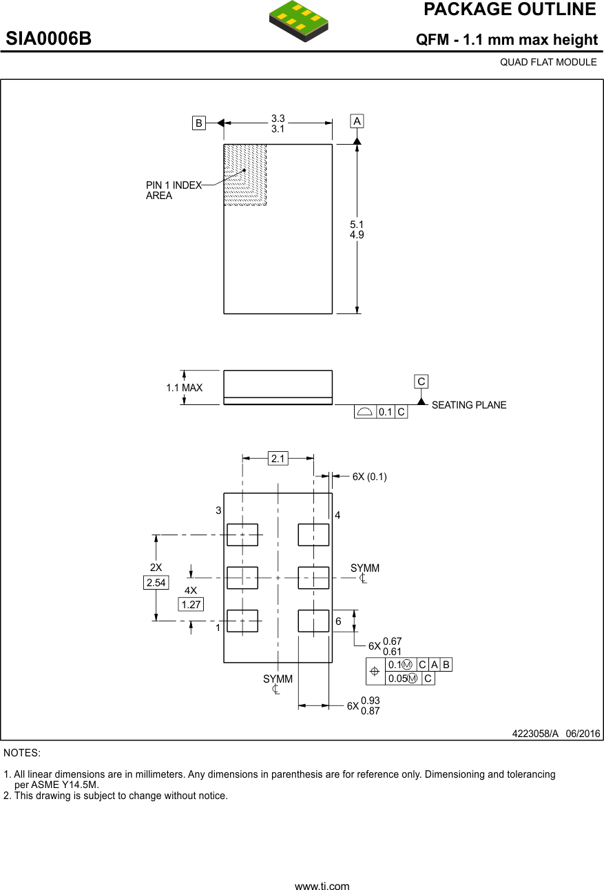
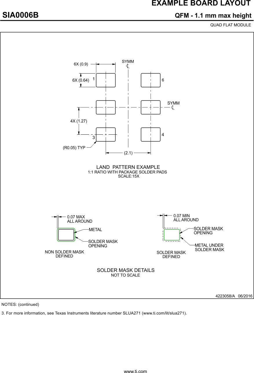
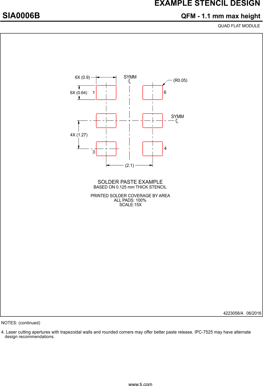
10 Mechanical, Packaging, and Orderable Information
The following pages include mechanical, packaging, and orderable information. This information is the most current data available for the designated devices. This data is subject to change without notice and revision of this document. For browser-based versions of this data sheet, refer to the left-hand navigation.


