ZHCSGL4C June   2017  – April 2019 LMX2595

PRODUCTION DATA.  

  1. 特性
  2. 应用
  3. 说明
    1.     Device Images
      1.      简化原理图
  4. 修订历史记录
  5. Pin Configuration and Functions
    1.     Pin Functions
  6. Specifications
    1. 6.1 Absolute Maximum Ratings
    2. 6.2 ESD Ratings
    3. 6.3 Recommended Operating Conditions
    4. 6.4 Thermal Information
    5. 6.5 Electrical Characteristics
    6. 6.6 Timing Requirements
    7. 6.7 Typical Characteristics
  7. Detailed Description
    1. 7.1 Overview
    2. 7.2 Functional Block Diagram
    3. 7.3 Feature Description
      1. 7.3.1  Reference Oscillator Input
      2. 7.3.2  Reference Path
        1. 7.3.2.1 OSCin Doubler (OSC_2X)
        2. 7.3.2.2 Pre-R Divider (PLL_R_PRE)
        3. 7.3.2.3 Programmable Multiplier (MULT)
        4. 7.3.2.4 Post-R Divider (PLL_R)
        5. 7.3.2.5 State Machine Clock
      3. 7.3.3  PLL Phase Detector and Charge Pump
      4. 7.3.4  N-Divider and Fractional Circuitry
      5. 7.3.5  MUXout Pin
        1. 7.3.5.1 Lock Detect
        2. 7.3.5.2 Readback
      6. 7.3.6  VCO (Voltage-Controlled Oscillator)
        1. 7.3.6.1 VCO Calibration
        2. 7.3.6.2 Determining the VCO Gain
      7. 7.3.7  Channel Divider
      8. 7.3.8  VCO Doubler
      9. 7.3.9  Output Buffer
      10. 7.3.10 Power-Down Modes
      11. 7.3.11 Phase Synchronization
        1. 7.3.11.1 General Concept
        2. 7.3.11.2 Categories of Applications for SYNC
        3. 7.3.11.3 Procedure for Using SYNC
        4. 7.3.11.4 SYNC Input Pin
      12. 7.3.12 Phase Adjust
      13. 7.3.13 Fine Adjustments for Phase Adjust and Phase SYNC
      14. 7.3.14 Ramping Function
        1. 7.3.14.1 Manual Pin Ramping
          1. 7.3.14.1.1 Manual Pin Ramping Example
        2. 7.3.14.2 Automatic Ramping
          1. 7.3.14.2.1 Automatic Ramping Example (Triangle Wave)
      15. 7.3.15 SYSREF
        1. 7.3.15.1 Programmable Fields
        2. 7.3.15.2 Input and Output Pin Formats
          1. 7.3.15.2.1 Input Format for SYNC and SysRefReq Pins
          2. 7.3.15.2.2 SYSREF Output Format
        3. 7.3.15.3 Examples
        4. 7.3.15.4 SYSREF Procedure
      16. 7.3.16 SysRefReq Pin
    4. 7.4 Device Functional Modes
    5. 7.5 Programming
      1. 7.5.1 Recommended Initial Power-Up Sequence
      2. 7.5.2 Recommended Sequence for Changing Frequencies
      3. 7.5.3 General Programming Requirements
    6. 7.6 Register Maps
      1. 7.6.1  General Registers R0, R1, & R7
        1. Table 25. Field Descriptions
      2. 7.6.2  Input Path Registers
        1. Table 26. Field Descriptions
      3. 7.6.3  Charge Pump Registers (R13, R14)
        1. Table 27. Field Descriptions
      4. 7.6.4  VCO Calibration Registers
        1. Table 28. Field Descriptions
      5. 7.6.5  N Divider, MASH, and Output Registers
        1. Table 29. Field Descriptions
      6. 7.6.6  SYNC and SysRefReq Input Pin Register
        1. Table 30. Field Descriptions
      7. 7.6.7  Lock Detect Registers
        1. Table 31. Field Descriptions
      8. 7.6.8  MASH_RESET
        1. Table 32. Field Descriptions
      9. 7.6.9  SysREF Registers
        1. Table 33. Field Descriptions
      10. 7.6.10 CHANNEL Divider And VCO Doubler Registers
        1. Table 34. Field Descriptions
      11. 7.6.11 Ramping and Calibration Fields
        1. Table 35. Field Descriptions
      12. 7.6.12 Ramping Registers
        1. 7.6.12.1 Ramp Limits
          1. Table 36. Field Descriptions
        2. 7.6.12.2 Ramping Triggers, Burst Mode, and RAMP0_RST
          1. Table 37. Field Descriptions
        3. 7.6.12.3 Ramping Configuration
          1. Table 38. Field Descriptions
      13. 7.6.13 Readback Registers
        1. Table 39. Field Descriptions
  8. Application and Implementation
    1. 8.1 Application Information
      1. 8.1.1 OSCin Configuration
      2. 8.1.2 OSCin Slew Rate
      3. 8.1.3 RF Output Buffer Power Control
      4. 8.1.4 RF Output Buffer Pullup
      5. 8.1.5 Performance Comparison Between 1572 (0x0624) and 3115 (0x0C2B) for Register DBLR_IBIAS_CTRL1 (R25[15:0])
    2. 8.2 Typical Application
      1. 8.2.1 Design Requirements
      2. 8.2.2 Detailed Design Procedure
      3. 8.2.3 Application Curve
  9. Power Supply Recommendations
  10. 10Layout
    1. 10.1 Layout Guidelines
    2. 10.2 Layout Example
  11. 11器件和文档支持
    1. 11.1 器件支持
      1. 11.1.1 第三方米6体育平台手机版_好二三四免责声明
      2. 11.1.2 开发支持
    2. 11.2 文档支持
      1. 11.2.1 相关文档
    3. 11.3 接收文档更新通知
    4. 11.4 社区资源
    5. 11.5 商标
    6. 11.6 静电放电警告
    7. 11.7 术语表
  12. 12机械、封装和可订购信息

Performance Comparison Between 1572 (0x0624) and 3115 (0x0C2B) for Register DBLR_IBIAS_CTRL1 (R25[15:0])

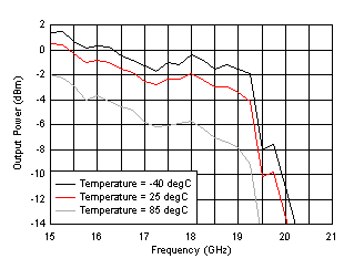
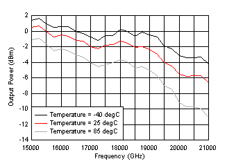
There is a new setting for register DBLR_IBIAS_CTRL1 (R25[15:0]): from 1572 (0x0624) to 3115 (0x0C2B). The old setting can operate up to 19-GHz output, but the new setting can extend the frequency range to 20 GHz. The field name DBLR_IBIAS_CTRL1 is short for "Doubler Current Bias Control 1". It only impacts the doubler and does not affect the performance below 15 GHz. Shown in Figure 57 and Figure 58, with old R25 value, the output power and phase noise floor fall apart beyond 19 GHz. But with the new setting, they remain stable up to 20 GHz. Figure 59 and Figure 60 show that new R25 value leads to less output power variation with temperature at high frequencies. Figure 61 shows the improvement in half harmonic.

LMX2595 D032_SNAS696.gif
OUTA_PWR = 20 Single-ended output
Figure 57. Phase Noise Floor Across Frequency: DBLR_IBIAS_CTRL1 (R25[15:0]) Value Old vs New
LMX2595 D028_SNAS696.gif
OUTA_PWR = 20 Single-ended output
Figure 59. Output Power Variation Versus Temperature: DBLR_IBIAS_CTRL1 = 1572
LMX2595 D033_SNAS696.gif
OUTA_PWR = 20 Single-ended output
Figure 61. 1/2 Harmonic Across Frequency: DBLR_IBIAS_CTRL1 (R25[15:0]) Value Old vs New
LMX2595 D029_SNAS696.gif
OUTA_PWR = 20 Single-ended output
Figure 58. Output Power Across Frequency: DBLR_IBIAS_CTRL1 (R25[15:0]) Value Old vs New
LMX2595 D034_SNAS696.gif
OUTA_PWR = 20 Single-ended output
Figure 60. Output Power Variation Versus Temperature: DBLR_IBIAS_CTRL1 = 3115