ZHCSGL5C March   2017  – April 2019 LMX2594

PRODUCTION DATA.  

  1. 特性
  2. 应用
  3. 说明
    1.     Device Images
      1.      简化原理图
  4. 修订历史记录
  5. Pin Configuration and Functions
    1.     Pin Functions
  6. Specifications
    1. 6.1 Absolute Maximum Ratings
    2. 6.2 ESD Ratings
    3. 6.3 Recommended Operating Conditions
    4. 6.4 Thermal Information
    5. 6.5 Electrical Characteristics
    6. 6.6 Timing Requirements
    7. 6.7 Typical Characteristics
  7. Detailed Description
    1. 7.1 Overview
    2. 7.2 Functional Block Diagram
    3. 7.3 Feature Description
      1. 7.3.1  Reference Oscillator Input
      2. 7.3.2  Reference Path
        1. 7.3.2.1 OSCin Doubler (OSC_2X)
        2. 7.3.2.2 Pre-R Divider (PLL_R_PRE)
        3. 7.3.2.3 Programmable Multiplier (MULT)
        4. 7.3.2.4 Post-R Divider (PLL_R)
        5. 7.3.2.5 State Machine Clock
      3. 7.3.3  PLL Phase Detector and Charge Pump
      4. 7.3.4  N-Divider and Fractional Circuitry
      5. 7.3.5  MUXout Pin
        1. 7.3.5.1 Lock Detect
        2. 7.3.5.2 Readback
      6. 7.3.6  VCO (Voltage-Controlled Oscillator)
        1. 7.3.6.1 VCO Calibration
        2. 7.3.6.2 Determining the VCO Gain
      7. 7.3.7  Channel Divider
      8. 7.3.8  Output Buffer
      9. 7.3.9  Power-Down Modes
      10. 7.3.10 Phase Synchronization
        1. 7.3.10.1 General Concept
        2. 7.3.10.2 Categories of Applications for SYNC
        3. 7.3.10.3 Procedure for Using SYNC
        4. 7.3.10.4 SYNC Input Pin
      11. 7.3.11 Phase Adjust
      12. 7.3.12 Fine Adjustments for Phase Adjust and Phase SYNC
      13. 7.3.13 Ramping Function
        1. 7.3.13.1 Manual Pin Ramping
          1. 7.3.13.1.1 Manual Pin Ramping Example
        2. 7.3.13.2 Automatic Ramping
          1. 7.3.13.2.1 Automatic Ramping Example (Triangle Wave)
      14. 7.3.14 SYSREF
        1. 7.3.14.1 Programmable Fields
        2. 7.3.14.2 Input and Output Pin Formats
          1. 7.3.14.2.1 Input Format for SYNC and SysRefReq Pins
          2. 7.3.14.2.2 SYSREF Output Format
        3. 7.3.14.3 Examples
        4. 7.3.14.4 SYSREF Procedure
      15. 7.3.15 SysRefReq Pin
    4. 7.4 Device Functional Modes
    5. 7.5 Programming
      1. 7.5.1 Recommended Initial Power-Up Sequence
      2. 7.5.2 Recommended Sequence for Changing Frequencies
      3. 7.5.3 General Programming Requirements
    6. 7.6 Register Maps
      1. 7.6.1  General Registers R0, R1, & R7
        1. Table 24. Field Descriptions
      2. 7.6.2  Input Path Registers
        1. Table 25. Field Descriptions
      3. 7.6.3  Charge Pump Registers (R13, R14)
        1. Table 26. Field Descriptions
      4. 7.6.4  VCO Calibration Registers
        1. Table 27. Field Descriptions
      5. 7.6.5  N Divider, MASH, and Output Registers
        1. Table 28. Field Descriptions
      6. 7.6.6  SYNC and SysRefReq Input Pin Register
        1. Table 29. Field Descriptions
      7. 7.6.7  Lock Detect Registers
        1. Table 30. Field Descriptions
      8. 7.6.8  MASH_RESET
        1. Table 31. Field Descriptions
      9. 7.6.9  SysREF Registers
        1. Table 32. Field Descriptions
      10. 7.6.10 CHANNEL Divider Registers
        1. Table 33. Field Descriptions
      11. 7.6.11 Ramping and Calibration Fields
        1. Table 34. Field Descriptions
      12. 7.6.12 Ramping Registers
        1. 7.6.12.1 Ramp Limits
          1. Table 35. Field Descriptions
        2. 7.6.12.2 Ramping Triggers, Burst Mode, and RAMP0_RST
          1. Table 36. Field Descriptions
        3. 7.6.12.3 Ramping Configuration
          1. Table 37. Field Descriptions
      13. 7.6.13 Readback Registers
        1. Table 38. Field Descriptions
  8. Application and Implementation
    1. 8.1 Application Information
      1. 8.1.1 OSCin Configuration
      2. 8.1.2 OSCin Slew Rate
      3. 8.1.3 RF Output Buffer Power Control
      4. 8.1.4 RF Output Buffer Pullup
    2. 8.2 Typical Application
      1. 8.2.1 Design Requirements
      2. 8.2.2 Detailed Design Procedure
      3. 8.2.3 Application Curve
  9. Power Supply Recommendations
  10. 10Layout
    1. 10.1 Layout Guidelines
    2. 10.2 Layout Example
  11. 11器件和文档支持
    1. 11.1 器件支持
      1. 11.1.1 第三方米6体育平台手机版_好二三四免责声明
      2. 11.1.2 开发支持
    2. 11.2 文档支持
      1. 11.2.1 相关文档
    3. 11.3 接收文档更新通知
    4. 11.4 社区资源
    5. 11.5 商标
    6. 11.6 静电放电警告
    7. 11.7 术语表
  12. 12机械、封装和可订购信息

Categories of Applications for SYNC

The requirements for SYNC depend on certain setup conditions. In cases that the SYNC is not timing critical, it can be done through software by toggling the VCO_PHASE_SYNC bit from 0 to 1. When it is timing critical, then it must be done through the pin and the setup and hold times for the OSCin pin are critical. Figure 27 gives the different categories.
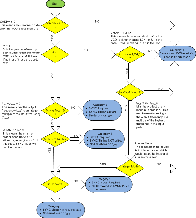
LMX2594 ai_sync_categories.gifFigure 27. Determining the SYNC Category