ZHCSGP5C August   2017  – February 2022 TIC12400-Q1

PRODUCTION DATA  

  1. 特性
  2. 应用
  3. 说明
  4. Revision History
  5. Pin Configuration and Functions
  6. Specifications
    1. 6.1 Absolute Maximum Ratings
    2. 6.2 ESD Ratings
    3. 6.3 Recommended Operating Conditions
    4. 6.4 Thermal Information
    5. 6.5 Electrical Characteristics
    6. 6.6 Timing Requirements
    7. 6.7 Typical Characteristics
  7. Parameter Measurement Information
  8. Detailed Description
    1. 8.1 Overview
    2. 8.2 Functional Block Diagram
    3. 8.3 Feature Description
      1. 8.3.1  VS Pin
      2. 8.3.2  VDD Pin
      3. 8.3.3  Device Initialization
      4. 8.3.4  Device Trigger
      5. 8.3.5  Device Reset
        1. 8.3.5.1 VS Supply POR
        2. 8.3.5.2 Hardware Reset
        3. 8.3.5.3 Software Reset
      6. 8.3.6  VS Under-Voltage (UV) Condition
      7. 8.3.7  VS Over-Voltage (OV) Condition
      8. 8.3.8  Switch Inputs Settings
        1. 8.3.8.1 Input Current Source and Sink Selection
        2. 8.3.8.2 Input Mode Selection
        3. 8.3.8.3 Input Enable Selection
        4. 8.3.8.4 Thresholds Adjustment
        5. 8.3.8.5 Wetting Current Configuration
      9. 8.3.9  Interrupt Generation and INT Assertion
        1. 8.3.9.1 INT Pin Assertion Scheme
        2. 8.3.9.2 Interrupt Idle Time (tINT_IDLE) Time
        3. 8.3.9.3 Microcontroller Wake-Up
        4. 8.3.9.4 Interrupt Enable or Disable and Interrupt Generation Conditions
        5. 8.3.9.5 Detection Filter
      10. 8.3.10 Temperature Monitor
        1. 8.3.10.1 Temperature Warning (TW)
        2. 8.3.10.2 Temperature Shutdown (TSD)
      11. 8.3.11 Parity Check and Parity Generation
      12. 8.3.12 Cyclic Redundancy Check (CRC)
    4. 8.4 Device Functional Modes
      1. 8.4.1 Continuous Mode
      2. 8.4.2 Polling Mode
        1. 8.4.2.1 Standard Polling
        2. 8.4.2.2 Matrix polling
      3. 8.4.3 Additional Features
        1. 8.4.3.1 Clean Current Polling (CCP)
        2. 8.4.3.2 Wetting Current Auto-Scaling
        3. 8.4.3.3 VS Measurement
        4. 8.4.3.4 Wetting Current Diagnostic
        5. 8.4.3.5 ADC Self-Diagnostic
    5. 8.5 Programming
      1. 8.5.1 SPI Communication Interface Buses
        1. 8.5.1.1 Chip Select ( CS)
        2. 8.5.1.2 System Clock (SCLK)
        3. 8.5.1.3 Slave In (SI)
        4. 8.5.1.4 Slave Out (SO)
      2. 8.5.2 SPI Sequence
        1. 8.5.2.1 Read Operation
        2. 8.5.2.2 Write Operation
        3. 8.5.2.3 Status Flag
    6. 8.6 Register Maps
    7. 8.7 Programming Guidelines
  9. Application Information Disclaimer
    1. 9.1 Application Information
    2. 9.2 Using TIC12400-Q1 in a 12 V Automotive System
    3. 9.3 Resistor-coded Switches Detection in Automotive Body Control Module
      1. 9.3.1 Design Requirements
      2. 9.3.2 Detailed Design Procedure
      3. 9.3.3 Application Curves
  10. 10Power Supply Recommendations
  11. 11Layout
    1. 11.1 Layout Guidelines
    2. 11.2 Layout Example
  12. 12Device and Documentation Support
    1. 12.1 接收文档更新通知
    2. 12.2 支持资源
    3. 12.3 Trademarks
    4. 12.4 Electrostatic Discharge Caution
    5. 12.5 术语表
  13. 13Mechanical, Packaging, and Orderable Information

Interrupt Generation and INT Assertion

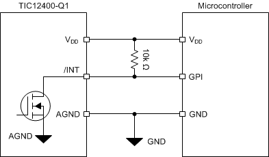
The INT pin is an active-low, open-drain output that asserts low when an event such as switch input state change, temperature warning, over-voltage shutdown, and so fourth, is detected by the TIC12400-Q1. An external pull-up resistor to VDD is needed on the INT pin (see Figure 8-4). The INT pin can also be connected directly to a 12 V automotive battery to support the microcontroller wake-up feature, as describe in Section 8.3.9.3.
GUID-BC66A24D-63AF-44CB-B2A4-C371AE63E3B0-low.gifFigure 8-4 INT Connection Example #1