ZHCSGP5C August 2017 – February 2022 TIC12400-Q1
PRODUCTION DATA
- 1 特性
- 2 应用
- 3 说明
- 4 Revision History
- 5 Pin Configuration and Functions
- 6 Specifications
- 7 Parameter Measurement Information
-
8 Detailed Description
- 8.1 Overview
- 8.2 Functional Block Diagram
- 8.3
Feature Description
- 8.3.1 VS Pin
- 8.3.2 VDD Pin
- 8.3.3 Device Initialization
- 8.3.4 Device Trigger
- 8.3.5 Device Reset
- 8.3.6 VS Under-Voltage (UV) Condition
- 8.3.7 VS Over-Voltage (OV) Condition
- 8.3.8 Switch Inputs Settings
- 8.3.9 Interrupt Generation and INT Assertion
- 8.3.10 Temperature Monitor
- 8.3.11 Parity Check and Parity Generation
- 8.3.12 Cyclic Redundancy Check (CRC)
- 8.4 Device Functional Modes
- 8.5 Programming
- 8.6 Register Maps
- 8.7 Programming Guidelines
- 9 Application Information Disclaimer
- 10Power Supply Recommendations
- 11Layout
- 12Device and Documentation Support
- 13Mechanical, Packaging, and Orderable Information
9.2 Using TIC12400-Q1 in a 12 V Automotive System
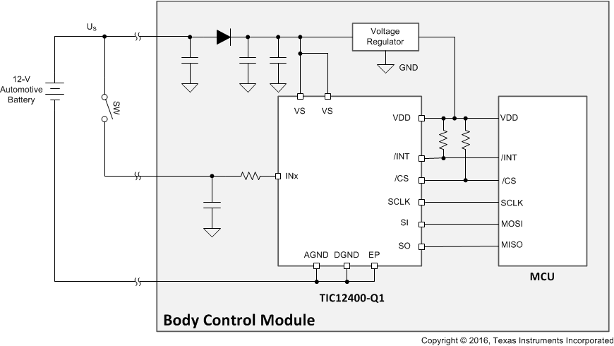
 Figure 9-1 Typical System Diagram of Battery Connections for TIC12400-Q1
The TIC12400-Q1 is designed to operate with a 12 V automotive system. Figure 9-1 depicts a typical system diagram to show how the device is connected to the battery. Remember to be careful when connecting the battery directly to the device on the VS supply pin (through a reverse-blocking diode) or the input (INX) pins since an automotive battery can be subjected to various transient and over-voltage events. Manufacturers have independently created standards and test procedures in an effort to prevent sensitive electronics from failing due to these events. Recently, combined efforts are made with ISO to develop the ISO 16750-2 standard (Road vehicles — Environmental conditions and testing for electrical and electronic equipment — Part 2: Electrical loads), which describe the possible transients that could occur to an automotive battery and specify test methods to simulate them.
It shall be noted that the TIC12400-Q1 is designed and tested according to the ISO 16750-2 standard. A few voltage stress tests and their test conditions are listed below. Exposing the device to more severe transient events than described by the standard could potentially causes performance degradation and long-term damage to the device.
- Direct current supply voltage: VBAT, min= 6 V; VBAT, max= 16 V
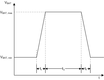
- To emulate a jump start event, voltage profile described in Figure 9-2 is used.
 Figure 9-2 Voltage Profile to Test a Jump Start EventTable 9-1 Voltage Profile Parameters to Test a Jump Start Event
Parameter Value VBAT, min 10.8 V VBAT, max 24 V tr < 10 ms t1 60 s ± 6 s tf < 10 ms Number of cycles 1 - To emulate a load dump event for an alternator with centralized load dump suppression, voltage profile described below is used. UA and US* are applied directly to VBAT. Figure 9-3 Voltage Profile to Test a Load Dump Event with Centralized Load Dump SuppressionTable 9-2 Voltage Profile Used to Test a Load Dump Event With Centralized Load Dump Suppression
Parameter Value UA 13.5 V US 79 V ≤ US ≤ 101 US* 35 V td 40 ms ≤ td ≤ 400 ms tr < 10 ms Number of cycles 5 pulses at intervals of 1 min - To emulate a cranking event, voltage profile describe below is used. US, US6, and UA are applied directly to VBAT. Figure 9-4 Voltage Profile to Test a Cranking EventTable 9-3 Voltage Profile Used to Test a Cranking Event
Parameter Value - Level I Value - Level II Value - Level IV US6 8 V 4.5 V 6 V US 9.5 V 6.5 V 6.5 V UB 14 V ± 0.2 V 14 V ± 0.2 V 14 V ± 0.2 V tf 5 ms ± 0.5 ms 5 ms ± 0.5 ms 5 ms ± 0.5 ms t6 15 ms ± 1.5 ms 15 ms ± 1.5 ms 15 ms ± 1.5 ms t7 50 ms ± 5 ms 50 ms ± 5 ms 50 ms ± 5 ms t8 1000 ms ± 100 ms 10000 ms ± 1000 ms 10000 ms ± 1000 ms tr 40 ms ± 4 ms 100 ms ± 10 ms 100 ms ± 10 ms