ZHCSGP5C August 2017 – February 2022 TIC12400-Q1
PRODUCTION DATA
- 1 特性
- 2 应用
- 3 说明
- 4 Revision History
- 5 Pin Configuration and Functions
- 6 Specifications
- 7 Parameter Measurement Information
-
8 Detailed Description
- 8.1 Overview
- 8.2 Functional Block Diagram
- 8.3
Feature Description
- 8.3.1 VS Pin
- 8.3.2 VDD Pin
- 8.3.3 Device Initialization
- 8.3.4 Device Trigger
- 8.3.5 Device Reset
- 8.3.6 VS Under-Voltage (UV) Condition
- 8.3.7 VS Over-Voltage (OV) Condition
- 8.3.8 Switch Inputs Settings
- 8.3.9 Interrupt Generation and INT Assertion
- 8.3.10 Temperature Monitor
- 8.3.11 Parity Check and Parity Generation
- 8.3.12 Cyclic Redundancy Check (CRC)
- 8.4 Device Functional Modes
- 8.5 Programming
- 8.6 Register Maps
- 8.7 Programming Guidelines
- 9 Application Information Disclaimer
- 10Power Supply Recommendations
- 11Layout
- 12Device and Documentation Support
- 13Mechanical, Packaging, and Orderable Information
8.3.6 VS Under-Voltage (UV) Condition
During normal operation of a typical 12 V automotive system, the VS voltage is usually quite stable and stays well above 11 V. However, the VS voltage may drop temporarily during certain vehicle operations, such as cold cranking. If the VS voltage drops below VUV_F, the TIC12400-Q1 enters the under-voltage (UV) condition since there is not enough voltage headroom for the device to accurately generate wetting currents. The following describes the behavior of the TIC12400-Q1 under UV condition:
- All current sources and sinks de-activate and switch monitoring stops.
- Interrupt is generated by asserting the INT pin low and the bit UV in the interrupt register (INT_STAT) is flagged to logic 1. The bit UV_STAT is asserted to logic 1 in the register IN_STAT_MISC. The OI SPI flag is asserted during any SPI transactions. The INT pin is released and the interrupt register (INT_STAT) is cleared on the rising edge of CS provided that the interrupt register has been read during the SPI transaction.
- SPI communication stays active, and all register settings stay intact without resetting. Previous switch status, if needed, can be retrieved without interruption.
- The device continues to monitor the VS voltage, and the UV condition sustains if the VS voltage continues to stay below VUV_R. No further interrupt is generated once cleared.
Note: the device resets as described in section VS Supply POR if the VS voltage drops below VPOR_F.
When the VS voltage rises above VUV_R, the INT pin is asserted low to notify the microcontroller that the UV condition no longer exists. The UV bit in the register INT_STAT is flagged to logic 1 and the bit UV_STAT bit is de-asserted to logic 0 in the register IN_STAT_MISC to reflect the clearance of the UV condition. The device resumes operation using current register settings (regardless of the INT pin and SPI communication status) with polling restarted from the first enabled channel. The Switch State Change (SSC) interrupt is generated at the end of the first polling cycle and the detected switch status becomes the baseline switch status for subsequent polling cycles. The content of the INT_STAT register, once read by the microcontroller, is cleared, and the INT pin is released afterwards.
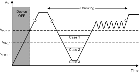
The following diagram describes the TIC12400-Q1 operation at various different VS voltages. If the VS voltage stays above VUV_F (Case 1), the device stays in normal operation. If the VS voltage drops below VUV_F but stays above VPOR_F (Case 2), the device enters the UV condition. If VS voltage drops below VPOR_F (Case 3), the device resets and all register settings are cleared. The microcontroller is then required to re-program all the configuration registers in order to resume normal operation after the VS voltage recovers.
 Figure 8-2 TIC12400-Q1 Operation at Various VS Voltage Levels