ZHCSGQ0A September 2017 – February 2022 TIC10024-Q1
PRODUCTION DATA
- 1 特性
- 2 应用
- 3 说明
- 4 Revision History
- 5 Pin Configuration and Functions
- 6 Specifications
- 7 Parameter Measurement Information
-
8 Detailed Description
- 8.1 Overview
- 8.2 Functional Block Diagram
- 8.3
Feature Description
- 8.3.1 VS Pin
- 8.3.2 VDD Pin
- 8.3.3 Device Initialization
- 8.3.4 Device Trigger
- 8.3.5 Device Reset
- 8.3.6 VS Under-Voltage (UV) Condition
- 8.3.7 VS Over-Voltage (OV) Condition
- 8.3.8 Switch Inputs Settings
- 8.3.9 Interrupt Generation and INT Assertion
- 8.3.10 Temperature Monitor
- 8.3.11 Parity Check And Parity Generation
- 8.3.12 Cyclic Redundancy Check (CRC)
- 8.4 Device Functional Modes
- 9 Programming
- 10Application and Implementation
- 11Power Supply Recommendations
- 12Layout
- 13Device and Documentation Support
- 14Mechanical, Packaging, and Orderable Information
8.4.3.2 Wetting Current Auto-Scaling
The 10 mA and 15 mA wetting current settings are useful to clean oxide build-up on the mechanical switch contact surface when the switch changes state from open to close. After the switch is closed, it is undesirable to keep the wetting current level at high level if only digital switches are monitored since it results in high current consumption and could potentially heat up the device quickly if multiple inputs are monitored. The wetting current auto-scaling feature helps mitigate this issue.
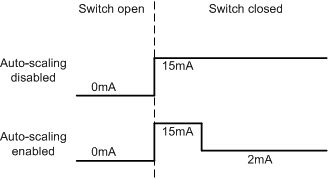
When enabled (AUTO_SCALE_DIS_CSO or AUTO_SCALE_DIS_CSI bit = logic 0 in the WC_CFG1 register), wetting current is reduced to 2 mA from 10 mA or 15 mA setting after switch closure is detected. The threshold used to determine a switch closure is the threshold configured in the THRES_COMP register.
The current reduction takes place N cycles after switch closure is detected on an input, where N depends on the setting of the DET_FILTER bits in the CONFIG register:
- DET_FILTER= 00: wetting current is reduced immediately in the next detection cycle after a closed switch is detected.
- DET_FILTER= 01: wetting current is reduced when a closed switch is detected and the switch status is stable for at least 2 consecutive detection cycles.
- DET_FILTER= 10: wetting current is reduced when a closed switch is detected and the switch status is stable for at least 3 consecutive detection cycles.
- DET_FILTER= 11: wetting current is reduced when a closed switch is detected and the switch status is stable for at least 4 consecutive detection cycles.
The wetting current is adjusted back to the original setting of 10 mA or 15 mA at a time of N cycles after an open switch is detected, where N again depends on the DET_FILTER bit setting in the CONFIG register. Figure 8-16 depicts the behavior of the wetting current auto-scaling feature.
 Figure 8-16 Wetting Current Auto-scaling Behavior
The wetting current auto-scaling only applies to 10 mA and 15 mA settings and is only available in continuous mode. If AUTO_SCALE_DIS_CSO or AUTO_SCALE_DIS_CSI bit is set to logic 1 in the WC_CFG1 registers, the wetting current stays at its original setting when a closed switch is detected. Power dissipation needs to be closely monitored when wetting current auto-scaling is disabled for multiple inputs as the device could heat up quickly when high wetting current settings are used. If the auto-scaling feature is disabled in continuous mode, the total power dissipation can be approximated using Equation 1.

where IWETT (TOTAL) is the sum of all wetting currents from all input channels. Increase in device junction temperature can be calculated based on P × RθJA. The junction temperature must be below TTSD for proper device operation. An interrupt will be issued when the junction temperature exceeds TTW or TTSD. For detailed description of the temperature monitoring, please refer to sections Temperature Warning (TW) and Temperature Shutdown (TSD).