ZHCSGQ7C September   2017  – May 2019 TDP142

PRODUCTION DATA.  

  1. 特性
  2. 应用
  3. 说明
    1.     Device Images
      1.      简化电路原理图
      2.      显示屏
  4. 修订历史记录
  5. Pin Configuration and Functions
    1.     Pin Functions
  6. Specifications
    1. 6.1  Absolute Maximum Ratings
    2. 6.2  ESD Ratings
    3. 6.3  Recommended Operating Conditions
    4. 6.4  Thermal Information
    5. 6.5  Power Supply Characteristics
    6. 6.6  DC Electrical Characteristics
    7. 6.7  AC Electrical Characteristics
    8. 6.8  Timing Requirements
    9. 6.9  Switching Characteristics
    10. 6.10 Typical Characteristics
  7. Parameter Measurement Information
  8. Detailed Description
    1. 8.1 Overview
    2. 8.2 Functional Block Diagram
    3. 8.3 Feature Description
      1. 8.3.1 DisplayPort
      2. 8.3.2 4-level Inputs
      3. 8.3.3 Receiver Linear Equalization
    4. 8.4 Device Functional Modes
      1. 8.4.1 Device Configuration in GPIO Mode
      2. 8.4.2 Device Configuration In I2C Mode
      3. 8.4.3 Linear EQ Configuration
      4. 8.4.4 Operation Timing – Power Up
    5. 8.5 Programming
    6. 8.6 Register Maps
      1. 8.6.1 General Register (address = 0x0A) [reset = 00000001]
        1. Table 6. General Registers
      2. 8.6.2 DisplayPort Control/Status Registers (address = 0x10) [reset = 00000000]
        1. Table 7. DisplayPort Control/Status Registers (0x10)
      3. 8.6.3 DisplayPort Control/Status Registers (address = 0x11) [reset = 00000000]
        1. Table 8. DisplayPort Control/Status Registers (0x11)
      4. 8.6.4 DisplayPort Control/Status Registers (address = 0x12) [reset = 00000000]
        1. Table 9. DisplayPort Control/Status Registers (0x12)
      5. 8.6.5 DisplayPort Control/Status Registers (address = 0x13) [reset = 00000000]
        1. Table 10. DisplayPort Control/Status Registers (0x13)
  9. Application and Implementation
    1. 9.1 Application Information
    2. 9.2 Typical Application
      1. 9.2.1 Source Application Implementation
        1. 9.2.1.1 Design Requirement
        2. 9.2.1.2 Detail Design Procedure
      2. 9.2.2 Sink Application Implementation
        1. 9.2.2.1 Design Requirements
        2. 9.2.2.2 Detailed Design Procedure
      3. 9.2.3 Application Curve
  10. 10Power Supply Recommendations
  11. 11Layout
    1. 11.1 Layout Guidelines
    2. 11.2 Layout Example
  12. 12器件和文档支持
    1. 12.1 相关链接
    2. 12.2 接收文档更新通知
    3. 12.3 社区资源
    4. 12.4 商标
    5. 12.5 静电放电警告
    6. 12.6 Glossary
  13. 13机械、封装和可订购信息

Source Application Implementation

Figure 18 shows the schematic for the Source side application. The TDP142 is placed between the DisplayPort Graphics Processor Unit (GPU) and the DisplayPort receptacle. The TDP142 monitors AUX traffic for power management purposes when SNOOPENZ is low.
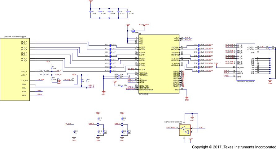
TDP142 sllsez1_app_source.gifFigure 18. The Block Diagram of DisplayPort Source Application