ZHCSGV0F July   2017  – December 2021 TPS22916

PRODUCTION DATA  

  1. 特性
  2. 应用
  3. 说明
  4. Revision History
  5. Pin Configuration and Functions
  6. Specifications
    1. 6.1 Absolute Maximum Ratings
    2. 6.2 ESD Ratings
    3. 6.3 Recommended Operating Conditions
    4. 6.4 Thermal Information
    5. 6.5 Electrical Characteristics
    6. 6.6 Switching Characteristics
    7. 6.7 Typical Characteristics
      1. 6.7.1 Typical Electrical Characteristics
      2. 6.7.2 Typical Switching Characteristics
  7. Parameter Measurement Information
  8. Detailed Description
    1. 8.1 Overview
    2. 8.2 Functional Block Diagram
    3. 8.3 Feature Description
      1. 8.3.1 On and Off Control
      2. 8.3.2 Fall Time (tFALL) and Quick Output Discharge (QOD)
      3. 8.3.3 Full-Time Reverse Current Blocking
    4. 8.4 Device Functional Modes
  9. Application and Implementation
    1. 9.1 Application Information
    2. 9.2 Typical Application
      1. 9.2.1 Design Requirements
      2. 9.2.2 Detailed Design Procedure
        1. 9.2.2.1 Maximum Inrush Current
      3. 9.2.3 Application Curve
  10. 10Power Supply Recommendations
  11. 11Layout
    1. 11.1 Layout Guidelines
    2. 11.2 Layout Example
    3. 11.3 Thermal Considerations
  12. 12Device and Documentation Support
    1. 12.1 Documentation Support
      1. 12.1.1 Related Documentation
    2. 12.2 接收文档更新通知
    3. 12.3 支持资源
    4. 12.4 Trademarks
    5. 12.5 Electrostatic Discharge Caution
    6. 12.6 术语表
  13. 13Mechanical, Packaging, and Orderable Information
    1. 13.1 Tape and Reel Information

Pin Configuration and Functions

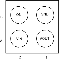
GUID-0A990257-3355-4617-B136-92A2B7D79721-low.gifFigure 5-1 YFP Package4-Pin WSONLaser Marking View
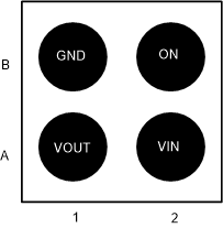
GUID-D4AE8EB6-5137-4D68-9E03-5984DC0403C0-low.gifFigure 5-2 YFP Package4-Pin WSONBump View
Table 5-1 Pin Functions
PIN TYPE DESCRIPTION
NO. NAME
A1 VOUT Power Switch output
A2 VIN Power Switch input
B1 GND Ground Device ground
B2 ON Digital input Device enable