ZHCSGV2J June 2009 – January 2017 OMAP-L138
PRODUCTION DATA.
- 1器件概述
- 2Revision History
-
3Device Comparison
- 3.1 Device Characteristics
- 3.2 Device Compatibility
- 3.3 ARM Subsystem
- 3.4 DSP Subsystem
- 3.5 Memory Map Summary
- 3.6 Pin Assignments
- 3.7 Pin Multiplexing Control
- 3.8
Terminal Functions
- 3.8.1 Device Reset, NMI and JTAG
- 3.8.2 High-Frequency Oscillator and PLL
- 3.8.3 Real-Time Clock and 32-kHz Oscillator
- 3.8.4 DEEPSLEEP Power Control
- 3.8.5 External Memory Interface A (EMIFA)
- 3.8.6 DDR2/mDDR Controller
- 3.8.7 Serial Peripheral Interface Modules (SPI)
- 3.8.8 Programmable Real-Time Unit (PRU)
- 3.8.9 Enhanced Capture/Auxiliary PWM Modules (eCAP0)
- 3.8.10 Enhanced Pulse Width Modulators (eHRPWM)
- 3.8.11 Boot
- 3.8.12 Universal Asynchronous Receiver/Transmitters (UART0, UART1, UART2)
- 3.8.13 Inter-Integrated Circuit Modules(I2C0, I2C1)
- 3.8.14 Timers
- 3.8.15 Multichannel Audio Serial Ports (McASP)
- 3.8.16 Multichannel Buffered Serial Ports (McBSP)
- 3.8.17 Universal Serial Bus Modules (USB0, USB1)
- 3.8.18 Ethernet Media Access Controller (EMAC)
- 3.8.19 Multimedia Card/Secure Digital (MMC/SD)
- 3.8.20 Liquid Crystal Display Controller(LCD)
- 3.8.21 Serial ATA Controller (SATA)
- 3.8.22 Universal Host-Port Interface (UHPI)
- 3.8.23 Universal Parallel Port (uPP)
- 3.8.24 Video Port Interface (VPIF)
- 3.8.25 General Purpose Input Output
- 3.8.26 Reserved and No Connect
- 3.8.27 Supply and Ground
- 3.9 Unused Pin Configurations
- 4Device Configuration
-
5Specifications
- 5.1 Absolute Maximum Ratings Over Operating Junction Temperature Range (Unless Otherwise Noted)
- 5.2 Handling Ratings
- 5.3 Recommended Operating Conditions
- 5.4 Notes on Recommended Power-On Hours (POH)
- 5.5 Electrical Characteristics Over Recommended Ranges of Supply Voltage and Operating Junction Temperature (Unless Otherwise Noted)
-
6Peripheral Information and Electrical Specifications
- 6.1 Parameter Information
- 6.2 Recommended Clock and Control Signal Transition Behavior
- 6.3 Power Supplies
- 6.4 Reset
- 6.5 Crystal Oscillator or External Clock Input
- 6.6 Clock PLLs
- 6.7 Interrupts
- 6.8 Power and Sleep Controller (PSC)
- 6.9 Enhanced Direct Memory Access Controller (EDMA3)
- 6.10 External Memory Interface A (EMIFA)
- 6.11
DDR2/mDDR Memory Controller
- 6.11.1 DDR2/mDDR Memory Controller Electrical Data/Timing
- 6.11.2 DDR2/mDDR Memory Controller Register Description(s)
- 6.11.3
DDR2/mDDR Interface
- 6.11.3.1 DDR2/mDDR Interface Schematic
- 6.11.3.2 Compatible JEDEC DDR2/mDDR Devices
- 6.11.3.3 PCB Stackup
- 6.11.3.4 Placement
- 6.11.3.5 DDR2/mDDR Keep Out Region
- 6.11.3.6 Bulk Bypass Capacitors
- 6.11.3.7 High-Speed Bypass Capacitors
- 6.11.3.8 Net Classes
- 6.11.3.9 DDR2/mDDR Signal Termination
- 6.11.3.10 VREF Routing
- 6.11.3.11 DDR2/mDDR CK and ADDR_CTRL Routing
- 6.11.3.12 DDR2/mDDR Boundary Scan Limitations
- 6.12 Memory Protection Units
- 6.13 MMC / SD / SDIO (MMCSD0, MMCSD1)
- 6.14 Serial ATA Controller (SATA)
- 6.15 Multichannel Audio Serial Port (McASP)
- 6.16
Multichannel Buffered Serial Port (McBSP)
- 6.16.1 McBSP Peripheral Register Description(s)
- 6.16.2
McBSP Electrical Data/Timing
- 6.16.2.1
Multichannel Buffered Serial Port (McBSP) Timing
- Table 6-59 Timing Requirements for McBSP0 [1.3V, 1.2V, 1.1V] (see )
- Table 6-60 Timing Requirements for McBSP0 [1.0V] (see )
- Table 6-61 Switching Characteristics for McBSP0 [1.3V, 1.2V, 1.1V] (see )
- Table 6-62 Switching Characteristics for McBSP0 [1.0V] (see )
- Table 6-63 Timing Requirements for McBSP1 [1.3V, 1.2V, 1.1V] (see )
- Table 6-64 Timing Requirements for McBSP1 [1.0V] (see )
- Table 6-65 Switching Characteristics for McBSP1 [1.3V, 1.2V, 1.1V] (see )
- Table 6-66 Switching Characteristics for McBSP1 [1.0V] (see )
- Table 6-67 Timing Requirements for McBSP0 FSR When GSYNC = 1 (see )
- Table 6-68 Timing Requirements for McBSP1 FSR When GSYNC = 1 (see )
- 6.16.2.1
Multichannel Buffered Serial Port (McBSP) Timing
- 6.17
Serial Peripheral Interface Ports (SPI0, SPI1)
- 6.17.1 SPI Peripheral Registers Description(s)
- 6.17.2
SPI Electrical Data/Timing
- 6.17.2.1
Serial Peripheral Interface (SPI) Timing
- Table 6-70 General Timing Requirements for SPI0 Master Modes
- Table 6-71 General Timing Requirements for SPI0 Slave Modes
- Table 6-78 General Timing Requirements for SPI1 Master Modes
- Table 6-79 General Timing Requirements for SPI1 Slave Modes
- Table 6-80 Additional SPI1 Master Timings, 4-Pin Enable Option
- Table 6-81 Additional SPI1 Master Timings, 4-Pin Chip Select Option
- 6.17.2.1
Serial Peripheral Interface (SPI) Timing
- 6.18 Inter-Integrated Circuit Serial Ports (I2C)
- 6.19 Universal Asynchronous Receiver/Transmitter (UART)
- 6.20 Universal Serial Bus OTG Controller (USB0) [USB2.0 OTG]
- 6.21 Universal Serial Bus Host Controller (USB1) [USB1.1 OHCI]
- 6.22 Ethernet Media Access Controller (EMAC)
- 6.23 Management Data Input/Output (MDIO)
- 6.24 LCD Controller (LCDC)
- 6.25 Host-Port Interface (UHPI)
- 6.26 Universal Parallel Port (uPP)
- 6.27 Video Port Interface (VPIF)
- 6.28 Enhanced Capture (eCAP) Peripheral
- 6.29 Enhanced High-Resolution Pulse-Width Modulator (eHRPWM)
- 6.30 Timers
- 6.31 Real Time Clock (RTC)
- 6.32 General-Purpose Input/Output (GPIO)
- 6.33 Programmable Real-Time Unit Subsystem (PRUSS)
- 6.34 Emulation Logic
- 7Device and Documentation Support
- 8Mechanical Packaging and Orderable Information
Table 6-112 Switching Characteristics Over Recommended Operating Conditions for LCD Raster Mode
See Figure 6-62 through Figure 6-66| NO. | PARAMETER | 1.3V, 1.2V, 1.1V | 1.0V | UNIT | |||
|---|---|---|---|---|---|---|---|
| MIN | MAX | MIN | MAX | ||||
| 1 | tc(PIXEL_CLK) | Cycle time, pixel clock | 26.66 | 33.33 | ns | ||
| 2 | tw(PIXEL_CLK_H) | Pulse duration, pixel clock high | 10 | 10 | ns | ||
| 3 | tw(PIXEL_CLK_L) | Pulse duration, pixel clock low | 10 | 10 | ns | ||
| 4 | td(LCD_D_V) | Delay time, LCD_PCLK high to LCD_D[15:0] valid (write) | 0 | 7 | 0 | 9 | ns |
| 5 | td(LCD_D_IV) | Delay time, LCD_PCLK high to LCD_D[15:0] invalid (write) | 0 | 7 | 0 | 9 | ns |
| 6 | td(LCD_AC_ENB_CS_A) | Delay time, LCD_PCLK low to LCD_AC_ENB_CS high | 0 | 7 | 0 | 9 | ns |
| 7 | td(LCD_AC_ENB_CS_I) | Delay time, LCD_PCLK low to LCD_AC_ENB_CS low | 0 | 7 | 0 | 9 | ns |
| 8 | td(LCD_VSYNC_A) | Delay time, LCD_PCLK low to LCD_VSYNC high | 0 | 7 | 0 | 9 | ns |
| 9 | td(LCD_VSYNC_I) | Delay time, LCD_PCLK low to LCD_VSYNC low | 0 | 7 | 0 | 9 | ns |
| 10 | td(LCD_HSYNC_A) | Delay time, LCD_PCLK high to LCD_HSYNC high | 0 | 7 | 0 | 9 | ns |
| 11 | td(LCD_HSYNC_I) | Delay time, LCD_PCLK high to LCD_HSYNC low | 0 | 7 | 0 | 9 | ns |
Frame-to-frame timing is derived through the following parameters in the LCD (RASTER_TIMING_1) register:
- Vertical front porch (VFP)
- Vertical sync pulse width (VSW)
- Vertical back porch (VBP)
- Lines per panel (LPP)
Line-to-line timing is derived through the following parameters in the LCD (RASTER_TIMING_0) register:
- Horizontal front porch (HFP)
- Horizontal sync pulse width (HSW)
- Horizontal back porch (HBP)
- Pixels per panel (PPL)
LCD_AC_ENB_CS timing is derived through the following parameter in the LCD (RASTER_TIMING_2) register:
- AC bias frequency (ACB)
The display format produced in raster mode is shown in Figure 6-62. An entire frame is delivered one line at a time. The first line delivered starts at data pixel (1, 1) and ends at data pixel (P, 1). The last line delivered starts at data pixel (1, L) and ends at data pixel (P, L). The beginning of each new frame is denoted by the activation of I/O signal LCD_VSYNC. The beginning of each new line is denoted by the activation of I/O signal LCD_HSYNC.
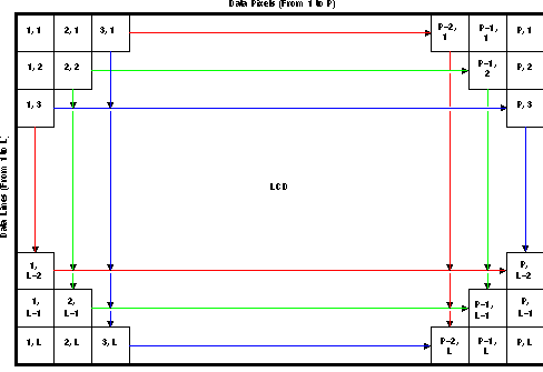 Figure 6-62 LCD Raster-Mode Display Format
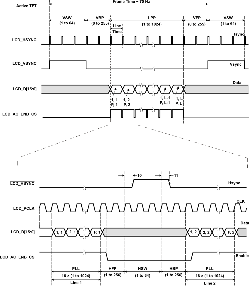 Figure 6-63 LCD Raster-Mode Active
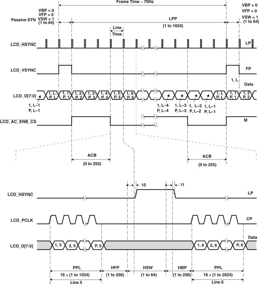 Figure 6-64 LCD Raster-Mode Passive
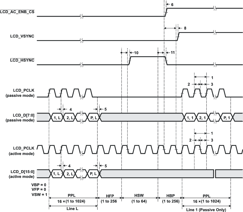 Figure 6-65 LCD Raster-Mode Control Signal Activation
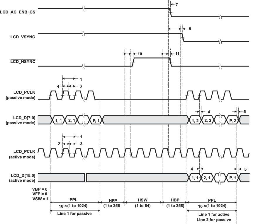 Figure 6-66 LCD Raster-Mode Control Signal Deactivation