ZHCSGY7B October   2017  – January 2018 TPS92830-Q1

PRODUCTION DATA.  

  1. 特性
  2. 应用
  3. 说明
    1.     简化原理图
  4. 修订历史记录
  5. 说明 (续)
  6. Pin Configuration and Functions
    1.     Pin Functions
  7. Specifications
    1. 7.1 Absolute Maximum Ratings
    2. 7.2 ESD Ratings
    3. 7.3 Recommended Operating Conditions
    4. 7.4 Thermal Information
    5. 7.5 Electrical Characteristics
    6. 7.6 Timing Requirements
    7. 7.7 Typical Characteristics
  8. Detailed Description
    1. 8.1 Overview
    2. 8.2 Functional Block Diagram
    3. 8.3 Feature Description
      1. 8.3.1 Device Bias
        1. 8.3.1.1 Power-On-Reset (POR)
        2. 8.3.1.2 Current Reference (IREF)
        3. 8.3.1.3 Low-Current Fault Mode
      2. 8.3.2 Charge Pump
        1. 8.3.2.1 Charge Pump Architecture
      3. 8.3.3 Constant-Current Driving
        1. 8.3.3.1 High-Side Current Sense
        2. 8.3.3.2 High-Side Current Driving
        3. 8.3.3.3 Gate Overdrive Voltage Protection
        4. 8.3.3.4 High-Precision Current Regulation
        5. 8.3.3.5 Parallel MOSFET Driving
      4. 8.3.4 PWM Dimming
        1. 8.3.4.1 Supply Dimming
        2. 8.3.4.2 PWM Dimming by Input
        3. 8.3.4.3 Internal Precision PWM Generator
        4. 8.3.4.4 Full Duty-Cycle Switch
      5. 8.3.5 Analog Dimming
        1. 8.3.5.1 Analog Dimming Topology
        2. 8.3.5.2 Internal High-Precision Pullup Current Source
      6. 8.3.6 Output Current Derating
        1. 8.3.6.1 Output-Current Derating Topology
      7. 8.3.7 Diagnostics and Fault
        1. 8.3.7.1 LED Short-to-GND Detection
        2. 8.3.7.2 LED Short-to-GND Auto Retry
        3. 8.3.7.3 LED Open-Circuit Detection
        4. 8.3.7.4 LED Open-Circuit Auto Retry
        5. 8.3.7.5 Dropout-Mode Diagnostics
        6. 8.3.7.6 Overtemperature Protection
        7. 8.3.7.7 FAULT Bus Output With One-Fails–All-Fail
        8. 8.3.7.8 Fault Table
    4. 8.4 Device Functional Modes
      1. 8.4.1 Undervoltage Lockout, V(IN) < V(UVLO)
      2. 8.4.2 Normal Operation (V(IN) ≥ 4.5 V, V(IN) > V(LED) + 0.5 V)
      3. 8.4.3 Low-Voltage Dropout
      4. 8.4.4 Fault Mode (Fault Is Detected)
  9. Application and Implementation
    1. 9.1 Application Information
    2. 9.2 Typical Applications
      1. 9.2.1 Typical Application for Automotive Exterior Lighting With One-Fails–All-Fail
        1. 9.2.1.1 Design Requirements
        2. 9.2.1.2 Detailed Design Procedure
        3. 9.2.1.3 Application Curves
      2. 9.2.2 High-Precision Dual-Brightness PWM Generation
        1. 9.2.2.1 Dual-Brightness Application
        2. 9.2.2.2 Design Requirements
        3. 9.2.2.3 Detailed Design Procedure
        4. 9.2.2.4 Application Curve
      3. 9.2.3 Driving High-Current LEDs With Parallel MOSFETs
        1. 9.2.3.1 Application Curves
  10. 10Layout
    1. 10.1 Layout Guidelines
    2. 10.2 Layout Example
  11. 11器件和文档支持
    1. 11.1 接收文档更新通知
    2. 11.2 社区资源
    3. 11.3 商标
    4. 11.4 静电放电警告
    5. 11.5 Glossary
  12. 12机械、封装和可订购信息

Charge Pump Architecture

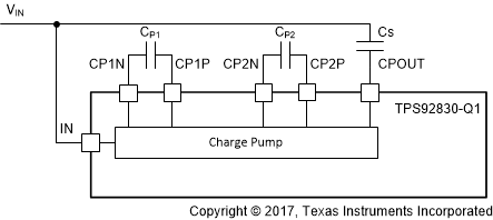
The TPS92830-Q1 device uses a two-stage charge pump to generate the high-side gate-drive voltage. The charge pump is a voltage tripler using external flying and storage capacitors.

CP1 is the first-stage flying capacitor, connected between CP1P and CP1N, which are the positive and negative nodes, respectively. CP2 is the second-stage flying capacitor, connected between CP2P and CP2N, which are the positive and negative nodes, respectively. CS is the storage capacitor, connected between CPOUT and IN. CS stores charge for the high-side gate driver.

The charge pump switches at frequency f(cp_sw) to optimize EMI performance.

Negative nodes CP1N and CP2N are driven by a 5-V driver, thus the maximum voltage on charge-pump output node CPOUT is approximately V(IN) + V(CP_drv). The charge pump voltage across storage capacitor CS is not dependent on V(IN).
TPS92830-Q1 Charge_Pump_SLIS178.gifFigure 20. Charge Pump